SBOS940A May 2019 – March 2020 OPA818
PRODUCTION DATA.
- 1 Features
- 2 Applications
- 3 Description
- 4 Revision History
- 5 Device Comparison Table
- 6 Pin Configuration and Functions
- 7 Specifications
- 8 Detailed Description
- 9 Application and Implementation
- 10Power Supply Recommendations
- 11Layout
- 12Device and Documentation Support
- 13Mechanical, Packaging, and Orderable Information
Package Options
Mechanical Data (Package|Pins)
- DRG|8
Thermal pad, mechanical data (Package|Pins)
- DRG|8
Orderable Information
9.1.1 Wideband, Non-Inverting Operation
The OPA818 provides a unique combination of high GBWP, low-input voltage noise, and the DC precision of a trimmed JFET-input stage to provide an exceptional high input impedance for a voltage-feedback amplifier. Its very high GBWP of 2.7 GHz can be used to either deliver high-signal bandwidths at high gains, or to extend the achievable bandwidth or gain in photodiode-transimpedance applications. To achieve the full performance of the OPA818, careful attention to printed circuit board (PCB) layout and component selection is required as discussed in the following sections of this data sheet.
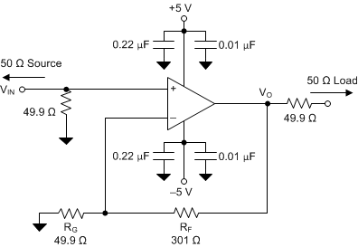
Figure 49 shows the non-inverting gain of +7 V/V circuit used as the basis for most of the Typical Characteristics: VS = ±5 V. Most of the curves were characterized using signal sources with 50-Ω driving impedance, and with measurement equipment presenting a 50-Ω load impedance. In Figure 49, the 49.9-Ω shunt resistor at the VIN terminal matches the source impedance of the test generator, while the 49.9-Ω series resistor at the VO terminal provides a matching resistor for the measurement equipment load. Generally, data sheet voltage swing specifications are at the output pin (VO in Figure 49) while output power specifications are at the matched 50-Ω load. The total 100-Ω load at the output combined with the 350-Ω total feedback network load, presents the OPA818 with an effective output load of 78 Ω for the circuit of Figure 49.
 Figure 49. Non-Inverting G = +7 V/V Configuration and Test Circuit
 Voltage-feedback operational amplifiers, unlike current feedback products, can use a wide range of resistor values to set their gain. To retain a controlled frequency response for the non-inverting voltage amplifier of Figure 49, the parallel combination of RF || RG should always be less than 50-Ω. In the non-inverting configuration, the parallel combination of RF || RG will form a pole with the parasitic input capacitance at the inverting node of the OPA818 (including layout parasitics). For best performance, this pole should be at a frequency greater than the closed loop bandwidth for the OPA818.