SBOS867D August 2017 – September 2024 OPA838
PRODMIX
- 1
- 1 Features
- 2 Applications
- 3 Description
- 4 Device Comparison Table
- 5 Pin Configuration and Functions
-
6 Specifications
- 6.1 Absolute Maximum Ratings
- 6.2 ESD Ratings
- 6.3 Recommended Operating Conditions
- 6.4 Thermal Information
- 6.5 Electrical Characteristics VS = 5 V
- 6.6 Electrical Characteristics VS = 3 V
- 6.7 Typical Characteristics: VS = 5 V
- 6.8 Typical Characteristics: VS = 3 V
- 6.9 Typical Characteristics: Over Supply Range
- 7 Detailed Description
- 8 Application and Implementation
- 9 Device and Documentation Support
- 10Revision History
- 11Mechanical, Packaging, and Orderable Information
Package Options
Refer to the PDF data sheet for device specific package drawings
Mechanical Data (Package|Pins)
- DBV|6
- DCK|5
- DCK|6
- DXB|8
Thermal pad, mechanical data (Package|Pins)
Orderable Information
7.4.2 Single-Supply Operation (2.7 V to 5.4 V)
Most newer systems use a single power supply to improve efficiency and to simplify power supply design. The OPA838 can be used with single-supply power (ground for the negative supply) with no change in performance from split supply, as long as the input and output pins are biased within the linear operating region of the device. The outputs nominally swing rail-to-rail with approximately a 100-mV headroom required for linear operation. The inputs can swing below the negative rail (typically ground) and to within 1.3 V of the positive supply. For dc-coupled, single-supply operation, the higher-gain operating applications typical of a decompensated op amp keep the input swings less than the input swing limit to the positive supply. Typically, the 1.3-V input headroom required to the positive supply does not limit operation.
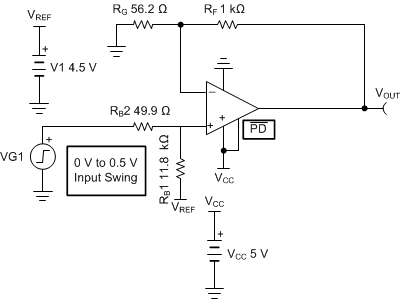
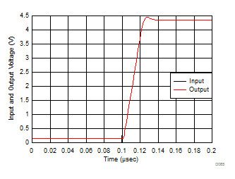
Figure 7-10 shows an example design that takes a 0‑V to 0.5‑V input range, level shifts the output up to 0.15 V for a 0‑V input using the 4.5‑V reference voltage common for 5‑V SAR ADCs, and sets the gain to produce a 4.1‑V output swing for the 0.5‑V input swing. This example assumes a 0‑Ω source that is required to sink the 39 µA required to bias the positive input pin to produce the 0.15‑V output for a 0‑V input. The RF and RG values are scaled down slightly to provide bias current cancellation by matching the parallel combination of the two bias set-up resistors on the noninverting input. Figure 7-11 illustrates an example step response for this circuit that produces an output from 0.15 V for a 0-V input to 4.35 V for a 0.5-V input.
 Figure 7-10 DC-Coupled, Single-Supply, Noninverting Interface With Output Level
Shift
 Figure 7-11 Unipolar Input to Level
Shifted Output Step Response
Figure 7-11 Unipolar Input to Level
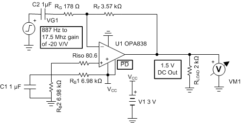
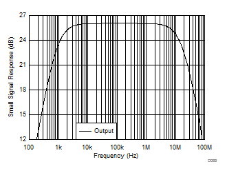
Shifted Output Step ResponseIf ac-coupling is acceptable, a simple way to operate single-supply is to run inverting. Figure 7-12 shows a low-power, high-gain example. In this example, a gain of –20 V/V is implemented (inverting usually does not matter for ac-coupled channels) where the V+ input is biased midscale. This example is showing an optional bias-current cancellation setup, which is not necessary unless the output dc level requires good accuracy. The parallel combination of the divider resistors plus the 80.7‑Ω isolating resistor match the feedback resistor value. With the blocking capacitor at the inverting input, the feedback resistor impedance must be matched to achieve bias current cancellation. In this 3-V supply example, the two inputs and the output are biased at 1.5 V. This places the input pins in range and centers the output for maximum V PP available. Figure 7-13 illustrates the small-signal response for this example showing a f–3dB range from a low-end cutoff of 887 Hz set by the input capacitor value to a 17.5-MHz high-frequency cutoff.
 Figure 7-12 Single-Supply Inverting Gain Stage With AC-Coupled Input
 Figure 7-13 Inverting
Single-Supply Response With AC-Coupled Input
Figure 7-13 Inverting
Single-Supply Response With AC-Coupled InputThese are only two of the many ways a single-supply design can be implemented. Many other methods exist, where using a dc reference voltage or ac-coupling are common. A good compilation of options can be found in Single-Supply Op Amp Design Techniques.