SBOS867D August   2017  – September 2024 OPA838

PRODMIX  

  1.   1
  2. Features
  3. Applications
  4. Description
  5. Device Comparison Table
  6. Pin Configuration and Functions
  7. Specifications
    1. 6.1 Absolute Maximum Ratings
    2. 6.2 ESD Ratings
    3. 6.3 Recommended Operating Conditions
    4. 6.4 Thermal Information
    5. 6.5 Electrical Characteristics VS = 5 V
    6. 6.6 Electrical Characteristics VS = 3 V
    7. 6.7 Typical Characteristics: VS = 5 V
    8. 6.8 Typical Characteristics: VS = 3 V
    9. 6.9 Typical Characteristics: Over Supply Range
  8. Detailed Description
    1. 7.1 Overview
    2. 7.2 Functional Block Diagram
    3. 7.3 Feature Description
      1. 7.3.1 Input Common-Mode Voltage Range
      2. 7.3.2 Output Voltage Range
      3. 7.3.3 Power-Down Operation
      4. 7.3.4 Trade-Offs in Selecting The Feedback Resistor Value
      5. 7.3.5 Driving Capacitive Loads
    4. 7.4 Device Functional Modes
      1. 7.4.1 Split-Supply Operation (±1.35 V to ±2.7 V)
      2. 7.4.2 Single-Supply Operation (2.7 V to 5.4 V)
      3. 7.4.3 Power Shutdown Operation
  9. Application and Implementation
    1. 8.1 Application Information
      1. 8.1.1 Noninverting Amplifier
      2. 8.1.2 Inverting Amplifier
      3. 8.1.3 Output DC Error Calculations
      4. 8.1.4 Output Noise Calculations
    2. 8.2 Typical Applications
      1. 8.2.1 High-Gain Differential I/O Designs
        1. 8.2.1.1 Design Requirements
        2. 8.2.1.2 Detailed Design Procedure
        3. 8.2.1.3 Application Curves
      2. 8.2.2 Transimpedance Amplifier
        1. 8.2.2.1 Design Requirements
        2. 8.2.2.2 Detailed Design Procedure
        3. 8.2.2.3 Application Curve
    3. 8.3 Power Supply Recommendations
    4. 8.4 Layout
      1. 8.4.1 Layout Guidelines
      2. 8.4.2 Layout Example
  10. Device and Documentation Support
    1. 9.1 Device Support
      1. 9.1.1 Development Support
        1. 9.1.1.1 TINA-TI™ Simulation Software (Free Download)
    2. 9.2 Documentation Support
      1. 9.2.1 Related Documentation
    3. 9.3 Receiving Notification of Documentation Updates
    4. 9.4 Support Resources
    5. 9.5 Trademarks
    6. 9.6 Electrostatic Discharge Caution
    7. 9.7 Glossary
  11. 10Revision History
  12. 11Mechanical, Packaging, and Orderable Information

Package Options

Refer to the PDF data sheet for device specific package drawings

Mechanical Data (Package|Pins)
  • DBV|6
  • DCK|5
  • DCK|6
  • DXB|8
Thermal pad, mechanical data (Package|Pins)
Orderable Information

Typical Characteristics: Over Supply Range

at PD = VS+ and TA = 25°C (unless otherwise noted)
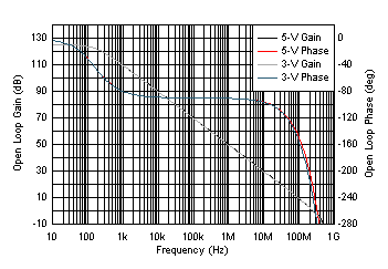
OPA838 Open-Loop Gain and Phase
No load, simulation
Figure 6-37 Open-Loop Gain and Phase
OPA838 Input
                        Spot Noise Density
 
Figure 6-39 Input Spot Noise Density
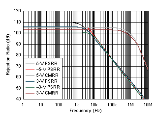
OPA838 PSRR and CMRR
Simulated results
Figure 6-41 PSRR and CMRR
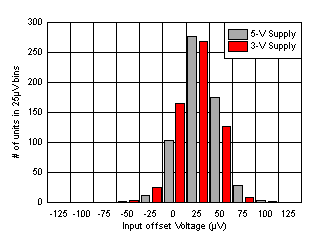
OPA838 Input Offset Voltage Distribution
600 units at each supply voltage
Figure 6-43 Input Offset Voltage Distribution
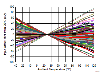
OPA838 Input
                        Offset Voltage vs Temperature
51 units at 5-V and 3-V supply
Figure 6-45 Input Offset Voltage vs Temperature
OPA838 Input Offset Voltage Drift Distribution
51 units at each supply
Figure 6-47 Input Offset Voltage Drift Distribution
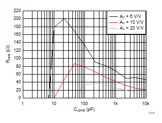
OPA838 Output Resistor vs CLOAD
See Figure 7-6 and Table 8-1
small signal, targeting 30° phase margin
Figure 6-49 Output Resistor vs CLOAD
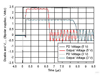
OPA838 Turn-On Time to Sinusoidal Input
 
Figure 6-51 Turn-On Time to Sinusoidal Input
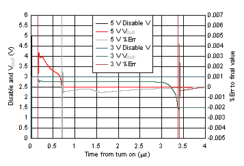
OPA838 Gain of 6-V/V Turn-On
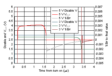
                        Time to Final DC Value at Midscale
Single-supply, DC input to produce midscale output (simulation)
Figure 6-53 Gain of 6-V/V Turn-On Time to Final DC Value at Midscale
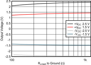
OPA838 Output Voltage Swing vs Load Resistor
 
Figure 6-55 Output Voltage Swing vs Load Resistor
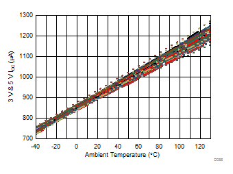
OPA838 Quiescent Current vs Temperature
 
Figure 6-57 Quiescent Current vs Temperature
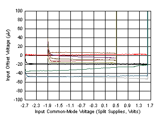
OPA838 Input
                        Offset Voltage vs Input Common-Mode Voltage
5 units, 3-V and 5-V supplies
Figure 6-59 Input Offset Voltage vs Input Common-Mode Voltage
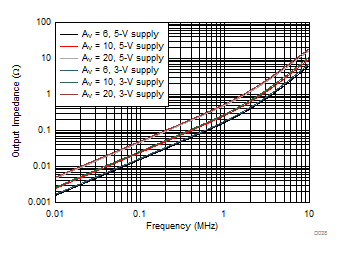
OPA838 Closed-Loop Output Impedance
See Figure 8-1 and Table 8-1 (simulation)
Figure 6-38 Closed-Loop Output Impedance
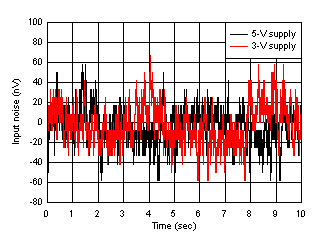
OPA838 Low-Frequency Voltage Noise
Input referred
Figure 6-40 Low-Frequency Voltage Noise
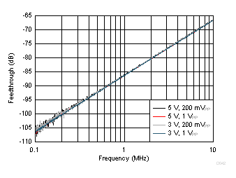
OPA838 Disabled Isolation Noninverting Input to Output
Measured, AV = 6 V/V, 100-Ω load
Figure 6-42 Disabled Isolation Noninverting Input to Output
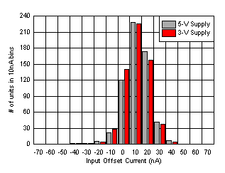
OPA838 Input Offset Current Distribution
600 units at each supply voltage
Figure 6-44 Input Offset Current Distribution
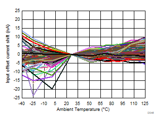
OPA838 Input
                        Offset Current vs Temperature
51 units at 5-V and 3-V supply
Figure 6-46 Input Offset Current vs Temperature
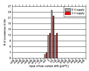
OPA838 Input Offset Current Drift Distribution
51 units at each supply
Figure 6-48 Input Offset Current Drift Distribution
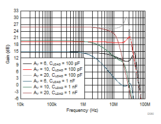
OPA838 Small-Signal Response Shapes vs CLOAD With Recommended ROUT
See Figure 7-6 and Table 8-1
2-kΩ parallel load to C LOAD
Figure 6-50 Small-Signal Response Shapes vs CLOAD With Recommended ROUT
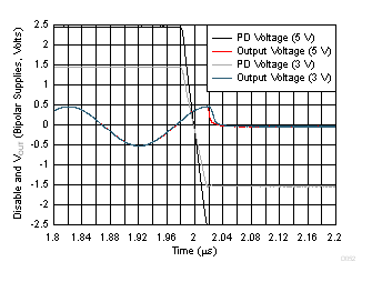
OPA838 Turn-Off Time to
                        Sinusoidal Input
 
Figure 6-52 Turn-Off Time to Sinusoidal Input
OPA838 Gain of 10-V/V Turn-On
                        Time to Final DC Value at Midscale
Single-supply, DC input to produce midscale output (simulation)
Figure 6-54 Gain of 10-V/V Turn-On Time to Final DC Value at Midscale
OPA838 Output Saturation Voltage vs Load Current
 
Figure 6-56 Output Saturation Voltage vs Load Current
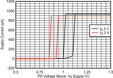
OPA838 Supply Current vs Power-Down Voltage: Turn On
                        Higher Than Turn Off
 
Figure 6-58 Supply Current vs Power-Down Voltage:
Turn On Higher Than Turn Off
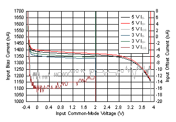
OPA838 Input
                        Bias and Offset Current vs VICM
Measured single device
Figure 6-60 Input Bias and Offset Current vs VICM