SBOS867D August 2017 – September 2024 OPA838
PRODMIX
- 1
- 1 Features
- 2 Applications
- 3 Description
- 4 Device Comparison Table
- 5 Pin Configuration and Functions
-
6 Specifications
- 6.1 Absolute Maximum Ratings
- 6.2 ESD Ratings
- 6.3 Recommended Operating Conditions
- 6.4 Thermal Information
- 6.5 Electrical Characteristics VS = 5 V
- 6.6 Electrical Characteristics VS = 3 V
- 6.7 Typical Characteristics: VS = 5 V
- 6.8 Typical Characteristics: VS = 3 V
- 6.9 Typical Characteristics: Over Supply Range
- 7 Detailed Description
- 8 Application and Implementation
- 9 Device and Documentation Support
- 10Revision History
- 11Mechanical, Packaging, and Orderable Information
Package Options
Refer to the PDF data sheet for device specific package drawings
Mechanical Data (Package|Pins)
- DBV|6
- DCK|5
- DCK|6
- DXB|8
Thermal pad, mechanical data (Package|Pins)
Orderable Information
8.2.1 High-Gain Differential I/O Designs
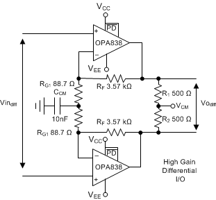
A high-gain differential-to-differential I/O circuit can be used to drive a second-stage FDA or a differential-to-single-ended stage. This circuit is frequently used in applications where high input impedance is required (for example, if the source cannot be loaded). Figure 8-3 illustrates an example design where the differential gain is 41 V/V. An added element between the two RG resistors increases the noise gain for the common-mode feedback. Make sure to provision for the added element; otherwise, a decompensated VFA (such as the OPA838) often oscillates. With only the RG elements in the differential I/O design, the common-mode feedback is unity-gain and often causes high-frequency, common-mode oscillations. To resolve this issue, split the RG elements in half and add a low-impedance path, such as a capacitor or a DC reference, between the two RG values.
 Figure 8-4 High-Gain Differential I/O Stage
Integrated results are available, but the OPA838 provides a low-power, high-frequency result. For best CMRR performance, match the resistors. A good rule is CMRR is approximately equal to the resistor tolerance; therefore, a 0.1% tolerance provides approximately 60-dB CMRR.