SBOS867D August 2017 – September 2024 OPA838
PRODMIX
- 1
- 1 Features
- 2 Applications
- 3 Description
- 4 Device Comparison Table
- 5 Pin Configuration and Functions
-
6 Specifications
- 6.1 Absolute Maximum Ratings
- 6.2 ESD Ratings
- 6.3 Recommended Operating Conditions
- 6.4 Thermal Information
- 6.5 Electrical Characteristics VS = 5 V
- 6.6 Electrical Characteristics VS = 3 V
- 6.7 Typical Characteristics: VS = 5 V
- 6.8 Typical Characteristics: VS = 3 V
- 6.9 Typical Characteristics: Over Supply Range
- 7 Detailed Description
- 8 Application and Implementation
- 9 Device and Documentation Support
- 10Revision History
- 11Mechanical, Packaging, and Orderable Information
Package Options
Refer to the PDF data sheet for device specific package drawings
Mechanical Data (Package|Pins)
- DBV|6
- DCK|5
- DCK|6
- DXB|8
Thermal pad, mechanical data (Package|Pins)
Orderable Information
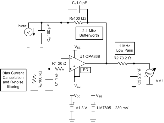
8.2.2 Transimpedance Amplifier
A common application for a high-gain-bandwidth voltage-feedback op amp is to amplify a small photodiode current from a capacitive detector. Figure 8-7 shows the front-page transimpedance circuit with more detail. Here, a fixed –0.23 negative voltage generator (LM7705) is used on the negative supply to make sure the output has adequate headroom when the output is at 0 V. The transimpedance stage is designed here for a 2.4‑MHz flat (Butterworth) response while a simple RC post-filter band-limits the broadband noise and sets the overall bandwidth to 1 MHz. The requirements for a high-dynamic-range transimpedance (or charge) amplifier include the very low input voltage noise intrinsic to a decompensated device like the OPA838. The noise gain over frequency for this type of circuit starts out at unity gain, and then begins to peak with a single zero response. This peaking is due to the pole formed in the feedback by the feedback resistor and the total capacitance on the inverting input. That noise gain response is flattened out at higher frequencies by the feedback capacitor value to be the 1 + CS / CF capacitor ratio. This noise gain is normally a very high, allowing the decompensated OPA838 to be applied to this application. The noise gain is intentionally peaked to a high value in this application; therefore, the very low input voltage noise (1.8 nV/√Hz) of the OPA838 improves dynamic range.
 Figure 8-7 100-kΩ Wide
Bandwidth Transimpedance Design