SBOS867D August 2017 – September 2024 OPA838
PRODMIX
- 1
- 1 Features
- 2 Applications
- 3 Description
- 4 Device Comparison Table
- 5 Pin Configuration and Functions
-
6 Specifications
- 6.1 Absolute Maximum Ratings
- 6.2 ESD Ratings
- 6.3 Recommended Operating Conditions
- 6.4 Thermal Information
- 6.5 Electrical Characteristics VS = 5 V
- 6.6 Electrical Characteristics VS = 3 V
- 6.7 Typical Characteristics: VS = 5 V
- 6.8 Typical Characteristics: VS = 3 V
- 6.9 Typical Characteristics: Over Supply Range
- 7 Detailed Description
- 8 Application and Implementation
- 9 Device and Documentation Support
- 10Revision History
- 11Mechanical, Packaging, and Orderable Information
Package Options
Refer to the PDF data sheet for device specific package drawings
Mechanical Data (Package|Pins)
- DBV|6
- DCK|5
- DCK|6
- DXB|8
Thermal pad, mechanical data (Package|Pins)
Orderable Information
8.1.2 Inverting Amplifier
The OPA838 can be used as an inverting amplifier with signal input to the inverting input (VIN–) through the gain-setting resistor (RG.) Figure 7-2 illustrates a basic block diagram of the circuit.
If VIN = VREF + VSIG, and the noninverting input is dc biased to VREF, the output of the amplifier is calculated according to Equation 2:
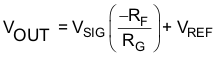
The signal gain of the circuit
 and VREF provides a reference
point around which the input and output signals swing. For bipolar-supply operation,
VREF is often GND. The output signal is 180° out-of-phase with the
input signal in the pass band of the application. Figure 8-2 illustrates the 50-Ω input matched configuration used for the inverting
characterization plots. In this case, an added termination resistor is placed in
parallel with the input RG resistor to provide an impedance match to 50-Ω
test equipment. Table 8-2 lists the suggested values for RF, RG, and RT
for inverting gains from –6 V/V to –20 V/V.
and VREF provides a reference
point around which the input and output signals swing. For bipolar-supply operation,
VREF is often GND. The output signal is 180° out-of-phase with the
input signal in the pass band of the application. Figure 8-2 illustrates the 50-Ω input matched configuration used for the inverting
characterization plots. In this case, an added termination resistor is placed in
parallel with the input RG resistor to provide an impedance match to 50-Ω
test equipment. Table 8-2 lists the suggested values for RF, RG, and RT
for inverting gains from –6 V/V to –20 V/V.
 Figure 8-2 Inverting With Input Impedance
Matching
Figure 8-2 Inverting With Input Impedance
Matching| AVERAGE | RF (Ω) | RG (Ω) | EXACT RT | STANDARD RT | INPUT ZI | ACTUAL (V/V) | GAIN (dB) |
|---|---|---|---|---|---|---|---|
| –6 | 1180 | 196 | 67.1 | 66.5 | 49.7 | –6.02 | 15.59 |
| –7 | 1370 | 196 | 67.1 | 66.5 | 49.7 | –6.99 | 16.89 |
| –8 | 1540 | 191 | 67.7 | 68.1 | 50.2 | –8.06 | 18.13 |
| –9 | 1690 | 187 | 68.2 | 68.1 | 49.9 | –9.04 | 19.12 |
| –10 | 1870 | 187 | 68.2 | 68.1 | 49.9 | –10 | 20 |
| –11 | 2050 | 187 | 68.2 | 68.1 | 49.9 | –10.96 | 20.80 |
| –12 | 2210 | 182 | 68.9 | 68.1 | 49.6 | –12.14 | 21.69 |
| –13 | 2370 | 182 | 68.9 | 68.1 | 49.6 | –13.02 | 22.29 |
| –14 | 2550 | 182 | 68.9 | 68.1 | 49.6 | –14.01 | 22.93 |
| –15 | 2740 | 182 | 68.9 | 68.1 | 49.6 | –15.05 | 23.55 |
| –16 | 2870 | 178 | 69.5 | 69.8 | 50.1 | –16.12 | 24.15 |
| –17 | 3090 | 182 | 68.9 | 69.8 | 50.5 | –16.98 | 24.6 |
| –18 | 3240 | 178 | 69.5 | 69.8 | 50.1 | –18.20 | 25.2 |
| –19 | 3400 | 178 | 69.5 | 69.8 | 50.1 | –19.10 | 25.62 |
| –20 | 3570 | 178 | 69.5 | 69.8 | 50.1 | –20.06 | 26.04 |