SBOS867D August   2017  – September 2024 OPA838

PRODMIX  

  1.   1
  2. Features
  3. Applications
  4. Description
  5. Device Comparison Table
  6. Pin Configuration and Functions
  7. Specifications
    1. 6.1 Absolute Maximum Ratings
    2. 6.2 ESD Ratings
    3. 6.3 Recommended Operating Conditions
    4. 6.4 Thermal Information
    5. 6.5 Electrical Characteristics VS = 5 V
    6. 6.6 Electrical Characteristics VS = 3 V
    7. 6.7 Typical Characteristics: VS = 5 V
    8. 6.8 Typical Characteristics: VS = 3 V
    9. 6.9 Typical Characteristics: Over Supply Range
  8. Detailed Description
    1. 7.1 Overview
    2. 7.2 Functional Block Diagram
    3. 7.3 Feature Description
      1. 7.3.1 Input Common-Mode Voltage Range
      2. 7.3.2 Output Voltage Range
      3. 7.3.3 Power-Down Operation
      4. 7.3.4 Trade-Offs in Selecting The Feedback Resistor Value
      5. 7.3.5 Driving Capacitive Loads
    4. 7.4 Device Functional Modes
      1. 7.4.1 Split-Supply Operation (±1.35 V to ±2.7 V)
      2. 7.4.2 Single-Supply Operation (2.7 V to 5.4 V)
      3. 7.4.3 Power Shutdown Operation
  9. Application and Implementation
    1. 8.1 Application Information
      1. 8.1.1 Noninverting Amplifier
      2. 8.1.2 Inverting Amplifier
      3. 8.1.3 Output DC Error Calculations
      4. 8.1.4 Output Noise Calculations
    2. 8.2 Typical Applications
      1. 8.2.1 High-Gain Differential I/O Designs
        1. 8.2.1.1 Design Requirements
        2. 8.2.1.2 Detailed Design Procedure
        3. 8.2.1.3 Application Curves
      2. 8.2.2 Transimpedance Amplifier
        1. 8.2.2.1 Design Requirements
        2. 8.2.2.2 Detailed Design Procedure
        3. 8.2.2.3 Application Curve
    3. 8.3 Power Supply Recommendations
    4. 8.4 Layout
      1. 8.4.1 Layout Guidelines
      2. 8.4.2 Layout Example
  10. Device and Documentation Support
    1. 9.1 Device Support
      1. 9.1.1 Development Support
        1. 9.1.1.1 TINA-TI™ Simulation Software (Free Download)
    2. 9.2 Documentation Support
      1. 9.2.1 Related Documentation
    3. 9.3 Receiving Notification of Documentation Updates
    4. 9.4 Support Resources
    5. 9.5 Trademarks
    6. 9.6 Electrostatic Discharge Caution
    7. 9.7 Glossary
  11. 10Revision History
  12. 11Mechanical, Packaging, and Orderable Information

Package Options

Refer to the PDF data sheet for device specific package drawings

Mechanical Data (Package|Pins)
  • DBV|6
  • DCK|5
  • DCK|6
  • DXB|8
Thermal pad, mechanical data (Package|Pins)
Orderable Information

Functional Block Diagram

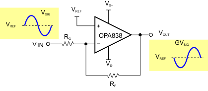
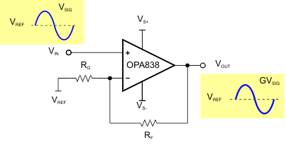
The OPA838 is a standard voltage-feedback op amp with two high-impedance inputs and a low-impedance output. Standard applications circuits are supported; see Figure 7-1 and Figure 7-2. These application circuits are shown with a dc VREF on the inputs that set the dc operating points for single-supply designs. The VREF is often ground, especially for split-supply applications.
OPA838 Noninverting AmplifierFigure 7-1 Noninverting Amplifier
OPA838 Inverting
                    Amplifier Figure 7-2 Inverting Amplifier