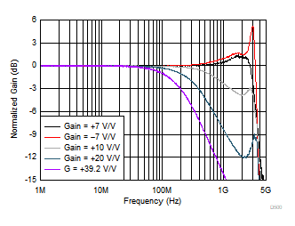
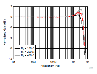
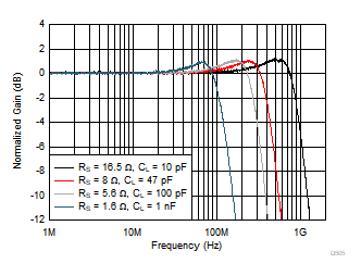
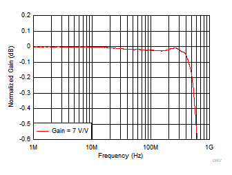
at TA = 25°C, VS+ = 2.5 V, VS– = –2.5 V, VIN+ = 0 V, RF = 453 Ω, Gain = 7 V/V, RL = 200 Ω, and output load referenced to midsupply (unless otherwise noted)

| VOUT = 100 mVPP; for circuit
configuration, see Section 8 |
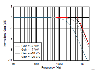
Figure 7-1 Small-Signal Frequency Response vs Gain Figure 7-3 Small-Signal Frequency Response vs Output Load
| VOUT = 100 mVPP; for circuit
configuration, see Figure 8-3 |
Figure 7-5 Small-Signal Frequency Response vs Capacitive Load Figure 7-7 Large-Signal Response for 0.1-dB Gain Flatness
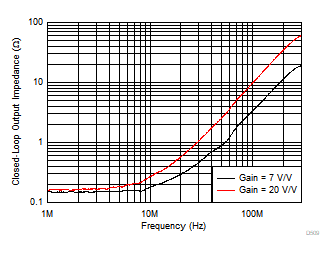
 Figure 7-9 Closed-Loop Output Impedance vs Frequency
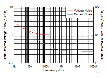
 Figure 7-11 Voltage and Current Noise Density vs Frequency
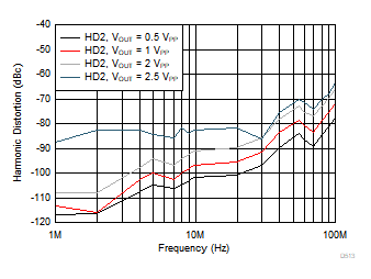
 Figure 7-13 Harmonic Distortion (HD2) vs Output Swing
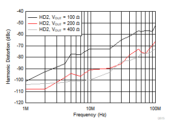
 Figure 7-15 Harmonic Distortion (HD2) vs Output Load
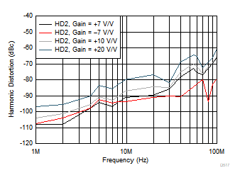
 Figure 7-17 Harmonic Distortion (HD2) vs Gain
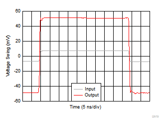
Average Rise and Fall Time (10% – 90%) = 300 ps
Rise and fall time limited
by test equipment |
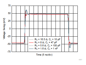
Figure 7-19 Small-Signal Transient Response Figure 7-21 Small-Signal Transient Response vs Capacitive Load
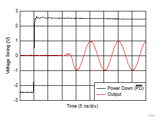
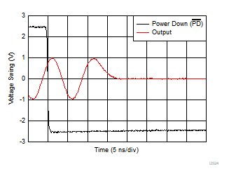
 Figure 7-23 Turnon Transient Response
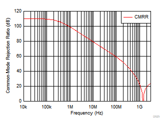
 Figure 7-25 Common-Mode Rejection Ratio vs Frequency
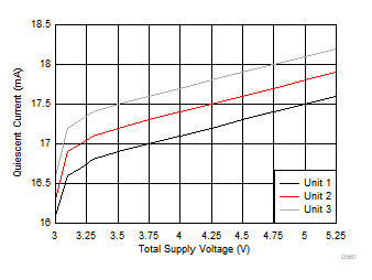
 Figure 7-27 Quiescent Current vs Supply Voltage
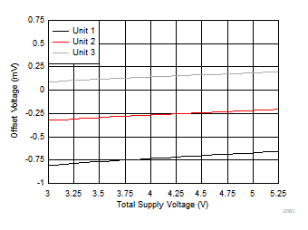
 Figure 7-29 Offset Voltage vs Supply Voltage
| VS+ = 5 V, VS– = 0 V |
3 Typical
Units |
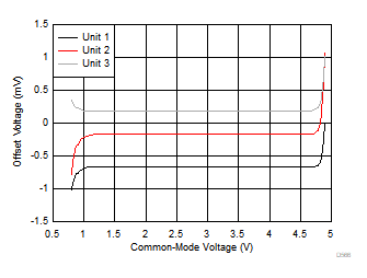
Figure 7-31 Offset Voltage vs Input Common-Mode Voltage
| VS+ = 5 V, VS– = 0 V |
3 Typical
Units |
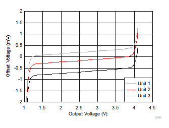
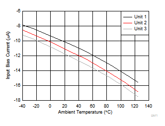
Figure 7-33 Offset Voltage vs Output Swing Figure 7-35 Input
Bias Current vs Ambient Temperature
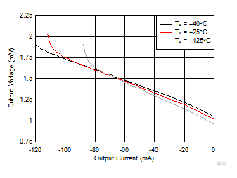
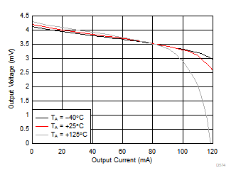
 Figure 7-37 Output Swing vs Sinking Current
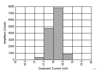
| µ = 17.6
mA |
σ = 0.3
mA |
13780 units
tested |
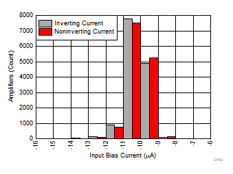
Figure 7-39 Quiescent Current Distribution
| µ = –11.2
µA |
σ = 0.6
µA |
13780 units
tested |
Figure 7-41 Input
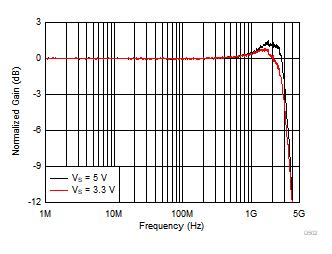
Bias Current Distribution Figure 7-2 Small-Signal Frequency Response vs Supply Voltage
| Gain = 39.2
V/V, RF = 953 Ω |
|
VOUT = 100 mVPP |
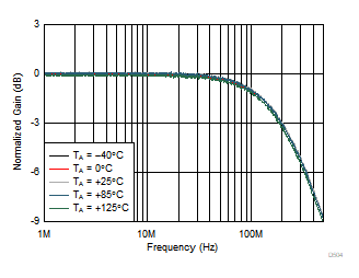
Figure 7-4 Small-Signal Frequency Response vs Ambient Temperature Figure 7-6 Large-Signal Frequency Response vs Gain
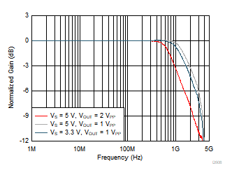
 Figure 7-8 Large-Signal Frequency Response vs Voltage Supply
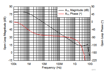
 Figure 7-10 Open-Loop Magnitude and Phase vs Frequency
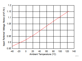
 Figure 7-12 Voltage Noise Density vs Ambient Temperature
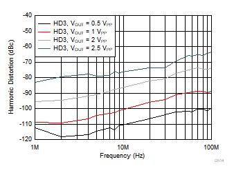
 Figure 7-14 Harmonic Distortion (HD3) vs Output Swing
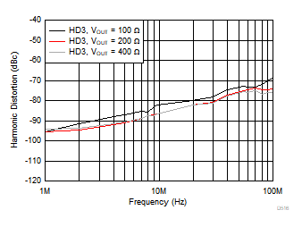
 Figure 7-16 Harmonic Distortion (HD3) vs Output Load
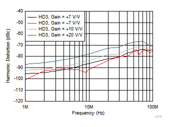
 Figure 7-18 Harmonic Distortion (HD3) vs Gain
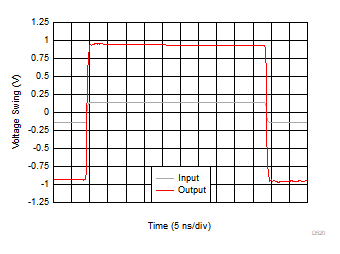
| Average Rise and Fall Time (10% – 90%) = 569 ps |
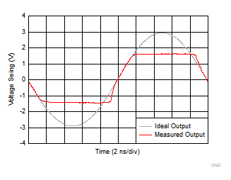
Figure 7-20 Large-Signal Transient Response Figure 7-22 Output Overload Response
 Figure 7-24 Turnoff Transient Response
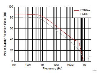
 Figure 7-26 Power
Supply Rejection Ratio vs Frequency
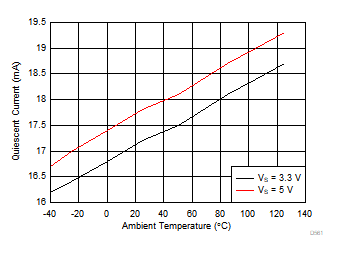
 Figure 7-28 Quiescent Current vs Ambient Temperature
| µ = 0.4
µV/°C |
σ = 0.7
µV/°C |
28 units
tested |
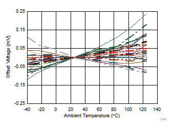
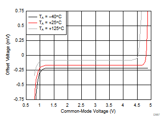
Figure 7-30 Offset Voltage vs Ambient Temperature Figure 7-32 Offset Voltage vs Input Common-Mode Voltage vs Ambient Temperature
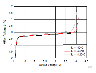
 Figure 7-34 Offset Voltage vs Output Swing vs Ambient Temperature
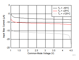
 Figure 7-36 Input
Bias Current vs Input Common-Mode Voltage vs Ambient Temperature
 Figure 7-38 Output Swing vs Sourcing Current
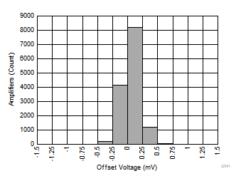
| µ = –0.2
mV |
σ = 0.15
mV |
13780 units
tested |
Figure 7-40 Offset Voltage Distribution
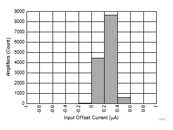
| µ = 0.04
µA |
σ = 0.1
µA |
13780 units
tested |
Figure 7-42 Input
Offset Current Distribution