SBOS622C July   2018  – January 2023 OPA855

PRODUCTION DATA  

  1. Features
  2. Applications
  3. Description
  4. Revision History
  5. Device Comparison Table
  6. Pin Configuration and Functions
  7. Specifications
    1. 7.1 Absolute Maximum Ratings
    2. 7.2 ESD Ratings
    3. 7.3 Thermal Information
    4. 7.4 Recommended Operating Conditions
    5. 7.5 Electrical Characteristics
    6. 7.6 Typical Characteristics
  8. Parameter Measurement Information
  9. Detailed Description
    1. 9.1 Overview
    2. 9.2 Functional Block Diagram
    3. 9.3 Feature Description
      1. 9.3.1 Input and ESD Protection
      2. 9.3.2 Feedback Pin
      3. 9.3.3 Wide Gain-Bandwidth Product
      4. 9.3.4 Slew Rate and Output Stage
    4. 9.4 Device Functional Modes
      1. 9.4.1 Split-Supply and Single-Supply Operation
      2. 9.4.2 Power-Down Mode
  10. 10Application, Implementation, and Layout
    1. 10.1 Application Information
    2. 10.2 Typical Application
      1. 10.2.1 Design Requirements
      2. 10.2.2 Detailed Design Procedure
      3. 10.2.3 Application Curves
    3. 10.3 Typical Application
      1. 10.3.1 Design Requirements
      2. 10.3.2 Detailed Design Procedure
      3. 10.3.3 Application Curves
    4. 10.4 Power Supply Recommendations
    5. 10.5 Layout
      1. 10.5.1 Layout Guidelines
      2. 10.5.2 Layout Example
  11. 11Device and Documentation Support
    1. 11.1 Device Support
      1. 11.1.1 Development Support
    2. 11.2 Documentation Support
      1. 11.2.1 Related Documentation
    3. 11.3 Receiving Notification of Documentation Updates
    4. 11.4 Support Resources
    5. 11.5 Trademarks
    6. 11.6 Electrostatic Discharge Caution
    7. 11.7 Glossary
  12. 12Mechanical, Packaging, and Orderable Information

Package Options

Mechanical Data (Package|Pins)
Thermal pad, mechanical data (Package|Pins)
Orderable Information

Input and ESD Protection

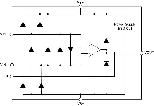
The OPA855 is fabricated on a low-voltage, high-speed, BiCMOS process. The internal, junction breakdown voltages are low for these small geometry devices, and as a result, all device pins are protected with internal ESD protection diodes to the power supplies as Figure 9-3 shows. There are two antiparallel diodes between the inputs of the amplifier that clamp the inputs during an overrange or fault condition.
GUID-9B9B0A8D-B619-430C-A5DF-B720765BEA87-low.gifFigure 9-3 Internal ESD Structure