SBOSA59 February 2021 OPA859-Q1
PRODUCTION DATA
- 1 Features
- 2 Applications
- 3 Description
- 4 Revision History
- 5 Pin Configuration and Functions
- 6 Specifications
- 7 Parameter Measurement Information
- 8 Detailed Description
- 9 Application and Implementation
- 10Power Supply Recommendations
- 11Layout
- 12Device and Documentation Support
- 13Mechanical, Packaging, and Orderable Information
Package Options
Mechanical Data (Package|Pins)
- DSG|8
Thermal pad, mechanical data (Package|Pins)
- DSG|8
Orderable Information
9.2 Typical Application
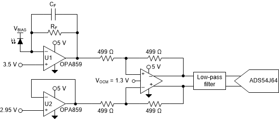
Figure 9-1 shows the OPA859-Q1 configured as a transimpedance amplifier (U1) in a wide-bandwidth, optical front-end system. A second OPA859-Q1 configured as a unity-gain buffer (U2) sets a dc offset voltage to the THS4520. The THS4520 is used to convert the single-ended transimpedance output of the OPA859-Q1 into a differential output signal. The THS4520 drives the input of the ADS54J64, 14-bit, 1-GSPS analog-to-digital converter (ADC) that digitizes the analog signal.
 Figure 9-1 OPA859-Q1 as
Both a TIA and a Buffer in an Optical Front-End System