SBOS919C August 2019 – August 2020 OPA862
PRODUCTION DATA
- 1 Features
- 2 Applications
- 3 Description
- 4 Revision History
- 5 Pin Configuration and Functions
-
6 Specifications
- 6.1 Absolute Maximum Ratings
- 6.2 ESD Ratings
- 6.3 Recommended Operating Conditions
- 6.4 Thermal Information
- 6.5 Electrical Characteristics: VS = ±2.5 V to ±5 V
- 6.6 Typical Characteristics: VS = ±5 V
- 6.7 Typical Characteristics: VS = ±2.5 V
- 6.8 Typical Characteristics: VS = 1.9 V, –1.4 V
- 6.9 Typical Characteristics: VS = 1.9 V, –1.4 V to ±5 V
- 7 Detailed Description
- 8 Application and Implementation
- 9 Power Supply Recommendations
- 10Layout
- 11Device and Documentation Support
- 12Mechanical, Packaging, and Orderable Information
Package Options
Mechanical Data (Package|Pins)
Thermal pad, mechanical data (Package|Pins)
Orderable Information
8.2.2.2 Detailed Design Procedure
In most TIA designs, selecting the right photodiode for the application is the most important decision because the photodiode determines the IIN and CD parameters that in turn determine the bandwidth required from the amplifier, the realizable TIA gain, and the signal bandwidth. Signal bandwidth also determines the rise time of the pulses. Choosing the photodiode with as low a capacitance as possible maximizes the TIA signal bandwidth for a given amplifier. Similarly, choosing a low TIA gain (RF) allows for higher signal bandwidth but having a RF as high as possible maximizes the SNR of the signal chain.
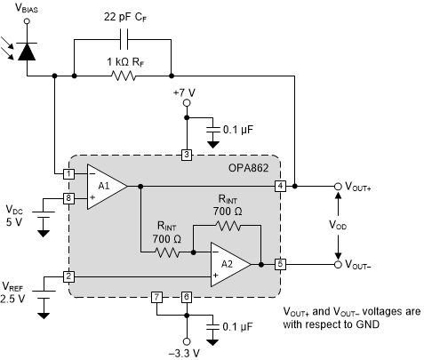
In order to take advantage of the increased SNR by using the OPA862 as described in Figure 8-5, the amplifier is already chosen. Using the design methodology explained at What You Need To Know About Transimpedance Amplifiers – Part 1 and the design parameters in Table 8-2, RF can be determined to be 1 kΩ and the required feedback capacitor, CF, is 22 pF. Because the range of IIN is 0 mA to 5 mA and RF is 1 kΩ, the range of a single-ended output voltage at VOUT+ is 0 V to 5 V (IIN × RF). In the cathode bias configuration of the photodiode condition in Figure 8-7, when the photodiode is excited the current flows towards VOUT+ through RF, resulting in a voltage pulse that goes lower from the zero current value. Thus, setting VOUT+ = 5 V and VOUT– = 0 V (VOD = +5 V) is desirable when the current is zero so that when the maximum current pulse of 5 mA occurs, VOUT+ goes to 0 V and VOUT– reaches 5 V (VOD = –5 V). The VOCM target of 2.5 V, which is a typical mid-reference voltage for differential input ADCs, can be set by choosing VREF = VOCM. The values of VDC and VREF can be determined by setting the values of VOUT+ and VOUT– to appropriate values at the zero photo-current in the following equations:
- VDC = VOUT+
- VREF = (VOUT– + VDC) / 2 = VOCM
Figure 8-8 and Figure 8-9 show the small-signal bandwidth and large-signal step response TINA simulation results of the circuit in Figure 8-7.
 Figure 8-7 TIA Circuit With the OPA862