SBOS919C August 2019 – August 2020 OPA862
PRODUCTION DATA
- 1 Features
- 2 Applications
- 3 Description
- 4 Revision History
- 5 Pin Configuration and Functions
-
6 Specifications
- 6.1 Absolute Maximum Ratings
- 6.2 ESD Ratings
- 6.3 Recommended Operating Conditions
- 6.4 Thermal Information
- 6.5 Electrical Characteristics: VS = ±2.5 V to ±5 V
- 6.6 Typical Characteristics: VS = ±5 V
- 6.7 Typical Characteristics: VS = ±2.5 V
- 6.8 Typical Characteristics: VS = 1.9 V, –1.4 V
- 6.9 Typical Characteristics: VS = 1.9 V, –1.4 V to ±5 V
- 7 Detailed Description
- 8 Application and Implementation
- 9 Power Supply Recommendations
- 10Layout
- 11Device and Documentation Support
- 12Mechanical, Packaging, and Orderable Information
Package Options
Mechanical Data (Package|Pins)
Thermal pad, mechanical data (Package|Pins)
Orderable Information
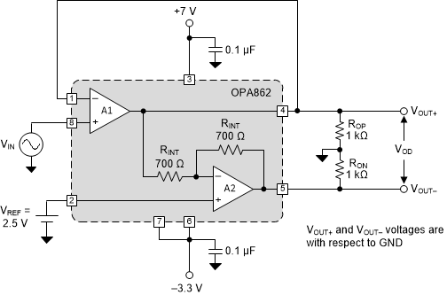
8.2.1 Single-Ended to Differential with 2.5-V Output Common-Mode Voltage
Most real-world signals are single ended. Often, fully differential amplifiers (FDAs) are used for single-ended-to-differential conversions but the low-impedance input of the FDA configuration can be a challenge for digital acquisition systems (DAQs). The high input impedance input of the OPA862, coupled with its ability to convert single-ended inputs to differential outputs, makes the device an excellent choice for DAQs.
 Figure 8-2 Single-Ended to Differential, G = 2 V/V With 2.5-V VOCM Configuration