SBOS919C August 2019 – August 2020 OPA862
PRODUCTION DATA
- 1 Features
- 2 Applications
- 3 Description
- 4 Revision History
- 5 Pin Configuration and Functions
-
6 Specifications
- 6.1 Absolute Maximum Ratings
- 6.2 ESD Ratings
- 6.3 Recommended Operating Conditions
- 6.4 Thermal Information
- 6.5 Electrical Characteristics: VS = ±2.5 V to ±5 V
- 6.6 Typical Characteristics: VS = ±5 V
- 6.7 Typical Characteristics: VS = ±2.5 V
- 6.8 Typical Characteristics: VS = 1.9 V, –1.4 V
- 6.9 Typical Characteristics: VS = 1.9 V, –1.4 V to ±5 V
- 7 Detailed Description
- 8 Application and Implementation
- 9 Power Supply Recommendations
- 10Layout
- 11Device and Documentation Support
- 12Mechanical, Packaging, and Orderable Information
Package Options
Mechanical Data (Package|Pins)
Thermal pad, mechanical data (Package|Pins)
Orderable Information
7.3.3 Precision and Low Noise
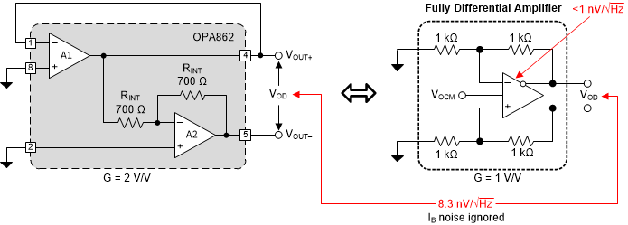
The OPA862 is laser trimmed for high DC precision. An important factor that reduces the DC precision of the system that uses the OPA862 is the errors introduced by the bias currents of A2 flowing through the internal feedback resistors, RINT; see Section 7.2. To minimize the error contribution from IB, the A2 amplifier of the OPA862 features a unique IB cancellation mechanism. This IB cancellation mechanism is the reason why the IB of A2 is orders of magnitude lower than the IB of A1. The DC errors are negligible for most applications because of the nanoamperes of IB and very low IB drift of A2. However, despite being very low, if the IB errors of A2 are significant for an application, a 348-Ω RREF resistor can be used on the VREF input to cancel out the IB errors. The tradeoff of using the RREF is that this resistor introduces noise that is amplified by a factor of two at VOUT– because of the noise gain of two of A2. The CFILT capacitor (see Section 7.2) also helps filter out the flat band noise contribution of RREF. The 700-Ω internal resistors were carefully chosen to balance low noise while keeping the total power dissipation low by taking advantage of the low 3.1-mA quiescent current of the OPA862. As shown in Figure 7-3, to get the equivalent 8.3-nV/√ Hz noise of the OPA862 with a typical FDA configuration, the FDA must be less than 1 nV/√ Hz; such FDAs are often difficult to find or expensive. When RREF equals 0 Ω, the typical error resulting from the IB of A2 appears as an input-referred offset of 3.5 µV at the VREF input, and when RREF is 348 Ω, the differential output-referred noise increases from 8.3 nV/√ Hz to 9.6 nV/√ Hz.
 Figure 7-3 Equivalent Voltage Noise FDA to OPA862