SBOS919C August 2019 – August 2020 OPA862
PRODUCTION DATA
- 1 Features
- 2 Applications
- 3 Description
- 4 Revision History
- 5 Pin Configuration and Functions
-
6 Specifications
- 6.1 Absolute Maximum Ratings
- 6.2 ESD Ratings
- 6.3 Recommended Operating Conditions
- 6.4 Thermal Information
- 6.5 Electrical Characteristics: VS = ±2.5 V to ±5 V
- 6.6 Typical Characteristics: VS = ±5 V
- 6.7 Typical Characteristics: VS = ±2.5 V
- 6.8 Typical Characteristics: VS = 1.9 V, –1.4 V
- 6.9 Typical Characteristics: VS = 1.9 V, –1.4 V to ±5 V
- 7 Detailed Description
- 8 Application and Implementation
- 9 Power Supply Recommendations
- 10Layout
- 11Device and Documentation Support
- 12Mechanical, Packaging, and Orderable Information
Package Options
Mechanical Data (Package|Pins)
Thermal pad, mechanical data (Package|Pins)
Orderable Information
3 Description
The OPA862 is a
single-ended to differential analog-to-digital converter
(ADC) driver with high input impedance for directly
interfacing with sensors. The device only consumes 3.1-mA
quiescent current for an output-referred noise density of
8.3 nV/√ Hz in a gain of 2-V/V
configuration. A fully differential amplifier configured in
a gain of 1 V/V with 1-kΩ resistors must be less than 1 nV/√
Hz to achieve the OPA862
equivalent output-referred noise density of
8.3 nV/√
Hz. The OPA862 can be
configured for other gains using external resistors. The
device has a large gain-bandwidth product of 400 MHz and a
slew rate of
140 V/µs. This
yields exceptional linearity and fast-settling, 18-bit
performance over comparable single-ended-to-differential ADC
drivers. The device includes a reference input pin for
setting the output common-mode voltage.
The OPA862 is fully characterized to operate over a wide supply range of 3 V to 12.6 V, and features a rail-to-rail output stage. The device is fabricated using Texas Instruments' proprietary, high-speed, silicon-germanium (SiGe) process and achieves exceptional distortion performance for 18-bit systems. The device includes a disable mode that consumes only 12-µA quiescent current in power-down state.
The OPA862 is rated to work over the extended industrial temperature range of –40°C to +125°C.
| PART NUMBER | PACKAGE | BODY SIZE (NOM) |
|---|---|---|
| OPA862 | SOIC (8) | 4.90 mm × 3.90 mm |
| WSON (8) | 3.00 mm × 3.00 mm |
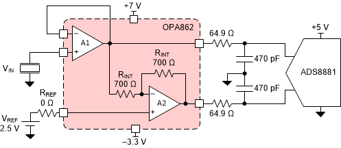
 Single-Ended
High-Input Impedance Sensor Interface
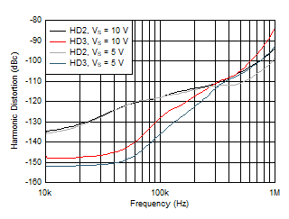
 Harmonic
Distortion vs Frequency