SBOS919C August   2019  – August 2020 OPA862

PRODUCTION DATA  

  1. Features
  2. Applications
  3. Description
  4. Revision History
  5. Pin Configuration and Functions
  6. Specifications
    1. 6.1 Absolute Maximum Ratings
    2. 6.2 ESD Ratings
    3. 6.3 Recommended Operating Conditions
    4. 6.4 Thermal Information
    5. 6.5 Electrical Characteristics: VS = ±2.5 V to ±5 V
    6. 6.6 Typical Characteristics: VS = ±5 V
    7. 6.7 Typical Characteristics: VS = ±2.5 V
    8. 6.8 Typical Characteristics: VS = 1.9 V, –1.4 V
    9. 6.9 Typical Characteristics: VS = 1.9 V, –1.4 V to ±5 V
  7. Detailed Description
    1. 7.1 Overview
    2. 7.2 Functional Block Diagram
    3. 7.3 Feature Description
      1. 7.3.1 Input and ESD Protection
      2. 7.3.2 Anti-Phase Reversal Protection
      3. 7.3.3 Precision and Low Noise
    4. 7.4 Device Functional Modes
      1. 7.4.1 Split-Supply Operation (±1.5 V to ±6.3 V)
      2. 7.4.2 Single-Supply Operation (3 V to 12.6 V)
  8. Application and Implementation
    1. 8.1 Application Information
      1. 8.1.1 Single-Ended-to-Differential Gain of 4 V/V
    2. 8.2 Typical Applications
      1. 8.2.1 Single-Ended to Differential with 2.5-V Output Common-Mode Voltage
        1. 8.2.1.1 Design Requirements
        2. 8.2.1.2 Detailed Design Procedure
        3. 8.2.1.3 Application Curves
      2. 8.2.2 Transimpedance Amplifier Configuration
        1. 8.2.2.1 Design Requirements
        2. 8.2.2.2 Detailed Design Procedure
        3. 8.2.2.3 Application Curves
      3. 8.2.3 DC Level-Shifting
  9. Power Supply Recommendations
  10. 10Layout
    1. 10.1 Layout Guidelines
    2. 10.2 Layout Examples
  11. 11Device and Documentation Support
    1. 11.1 Documentation Support
      1. 11.1.1 Related Documentation
    2. 11.2 Receiving Notification of Documentation Updates
    3. 11.3 Support Resources
    4. 11.4 Trademarks
    5. 11.5 Electrostatic Discharge Caution
    6. 11.6 Glossary
  12. 12Mechanical, Packaging, and Orderable Information

Package Options

Mechanical Data (Package|Pins)
Thermal pad, mechanical data (Package|Pins)
Orderable Information

Typical Characteristics: VS = ±5 V

TA ≈ 25°C, A1 input common-mode voltage (VCM) = midsupply, VREF = midsupply, RF (connected between
VOUT+ and VFB) = 0 Ω, RG = open, differential gain (G) = 2 V/V, RL (differential load) = 2 kΩ, and RREF = 0 Ω (unless otherwise noted).
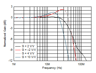
GUID-D109C259-53F1-47A3-9A8E-DFD81A14FF3C-low.gif
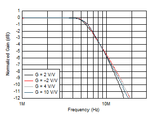
VOD = 20 mVPP
Figure 6-1 Small-Signal Frequency Response
GUID-4B49C4F7-CF02-498C-A8FE-AFE9D6BE5FE8-low.gif
Simulation
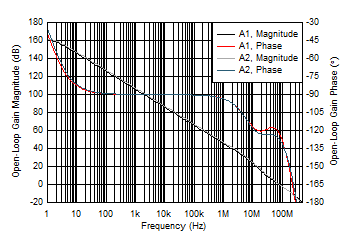
Figure 6-3 Open-Loop Gain And Phase vs Frequency
GUID-6AB9A028-149A-485C-BE2A-CFC6093792F4-low.gif
Simulation
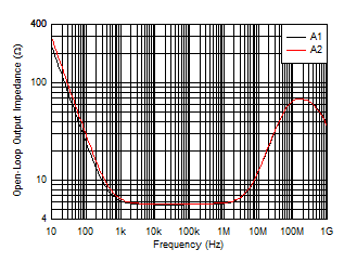
Figure 6-5 Open-Loop Output Impedance vs Frequency
GUID-D8013A34-3B80-40E5-AC3D-3C886CB9E762-low.gif
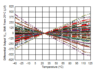
99 units
Figure 6-7 Differential Output Offset Voltage vs Temperature
GUID-1BE98CF0-1F8D-42B8-8865-E1C7FCA61971-low.gif
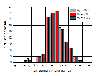
–40°C to +125°C, over 115 units
Figure 6-9 Differential Output Offset Voltage Drift Histogram
GUID-6D4D7C86-7C7A-4408-9AE1-6AFF22C13E2D-low.gif
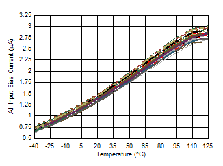
32 units
Figure 6-11 A1 Input Bias Current vs Temperature
GUID-04E671E3-14E9-479E-9F82-A592E58A1884-low.gif
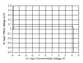
Figure 6-13 A1 Input Offset Voltage vs Input Common-Mode Voltage
GUID-AA7334C6-C1D2-4E74-A830-F74025A830EE-low.gif
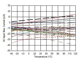
32 units
Figure 6-15 A2 Input Bias Current vs Temperature
GUID-2398790A-A708-442B-A9A9-EE35DD03E092-low.gif
Figure 6-17 Input Overdrive Recovery
GUID-AC09ABF7-5F9B-4C92-959B-855E98605717-low.gif
VOD = 10 VPP
Figure 6-2 Large-Signal Frequency Response
GUID-8D2D8142-9E65-442C-B67B-974913870081-low.gif
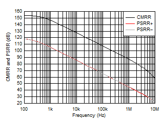
Simulation, A1 and A2
Figure 6-4 CMRR and PSRR vs Frequency
GUID-78DB671C-411B-4AB3-8178-CDFEF9F24145-low.gif
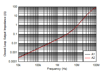
Simulation
Figure 6-6 Closed-Loop Output Impedance vs Frequency
GUID-445F3774-E5FF-4319-8D25-EF768D9862D0-low.gif
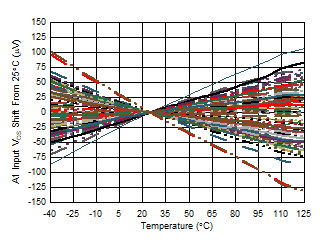
99 units
Figure 6-8 A1 Input Offset Voltage vs Temperature
GUID-6DE38E0F-DF93-48D8-BCBC-0364FD9C5C60-low.gif
–40°C to +125°C, over 115 units
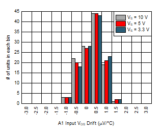
Figure 6-10 A1 Input Offset Voltage Drift Histogram
GUID-089FC202-D09F-4855-B384-1595EEFCFECE-low.gif
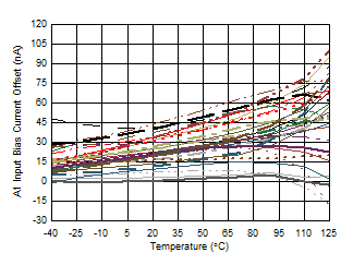
32 units
Figure 6-12 A1 Input Offset Current vs Temperature
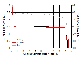
GUID-4A78DE1A-EB7A-46EE-BEA0-583B571B8A45-low.gif
Figure 6-14 A1 Input Bias Current and Input Offset Current vs Input Common-Mode Voltage
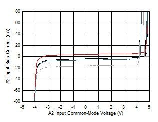
GUID-67442C6D-7CE3-43B6-A3C6-F7C287E57EEA-low.gif
Figure 6-16 A2 Input Bias Current vs Input Common-Mode Voltage
GUID-F90F6FA6-9A8C-4EF9-97DE-9B26BF184C0C-low.gif
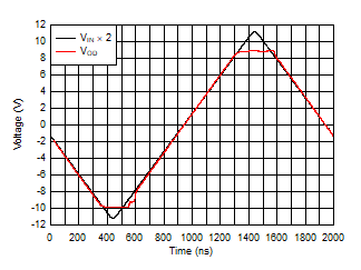
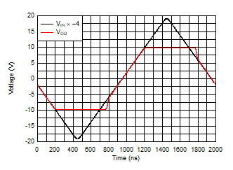
G = –4 V/V
Figure 6-18 Output Overdrive Recovery