SBOSA95F May 2022 – October 2024 OPA2863A , OPA863A
PRODUCTION DATA
- 1
- 1 Features
- 2 Applications
- 3 Description
- 4 Device Comparison Table
- 5 Pin Configuration and Functions
-
6 Specifications
- 6.1 Absolute Maximum Ratings
- 6.2 ESD Ratings
- 6.3 Recommended Operating Conditions
- 6.4 Thermal Information OPA863A
- 6.5 Thermal Information OPA2863A
- 6.6 Electrical Characteristics VS = ±5 V
- 6.7 Electrical Characteristics VS = 3 V
- 6.8 Typical Characteristics: VS = ±5 V
- 6.9 Typical Characteristics: VS = 3 V
- 6.10 Typical Characteristics: VS = 3 V to 10 V
- 7 Detailed Description
- 8 Application and Implementation
- 9 Device and Documentation Support
- 10Revision History
- 11Mechanical, Packaging, and Orderable Information
Package Options
Refer to the PDF data sheet for device specific package drawings
Mechanical Data (Package|Pins)
- DBV|5
Thermal pad, mechanical data (Package|Pins)
Orderable Information
7.3.3 ESD Protection
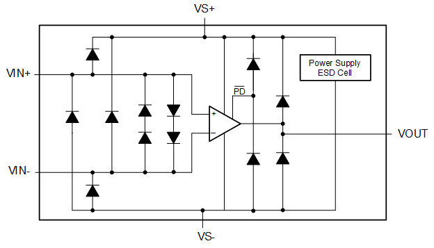
As Figure 7-1 shows, all device pins are protected with internal ESD protection diodes to the power supplies. These diodes provide moderate protection to input overdrive voltages greater than the supplies. The protection diodes typically support 10-mA continuous input and output currents. Use series current limiting resistors if input voltages exceeding the supply voltages occur at the amplifier inputs, which makes sure that the current through the ESD diodes remains within the rated value. OPAx863A is a bipolar amplifier; therefore, the two inputs are protected with antiparallel, back-to-back diodes between the inputs that limits the maximum input differential voltage to approximately 1 V. Make sure to use gain-setting and feedback resistors large enough to limit the current through these diodes in fast slewing conditions.
 Figure 7-1 Internal
ESD Protection