SLOSEB4A November 2023 – July 2024 OPA2892 , OPA892
PRODUCTION DATA
- 1
- 1 Features
- 2 Applications
- 3 Description
- 4 Pin Configuration and Functions
- 5 Specifications
- 6 Detailed Description
- 7 Application and Implementation
- 8 Device and Documentation Support
- 9 Revision History
- 10Mechanical, Packaging, and Orderable Information
Package Options
Refer to the PDF data sheet for device specific package drawings
Mechanical Data (Package|Pins)
- D|8
Thermal pad, mechanical data (Package|Pins)
Orderable Information
7.4.1.1 General PowerPAD™ Integrated Circuit Package Design Considerations
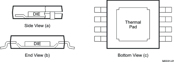
The OPAx892 is available in a thermally-enhanced DGN package, which is a member of the PowerPAD™ integrated circuit package family. Figure 7-7a and Figure 7-7b show that this package is constructed using a downset leadframe upon which the die is mounted. Figure 7-7c that this arrangement results in the leadframe being exposed as a thermal pad on the underside of the package. Because this thermal pad has direct thermal contact with the die, excellent thermal performance can be achieved by providing a good thermal path away from the thermal pad.
The PowerPAD integrated circuit package allows for both assembly and thermal management in one manufacturing operation. During the surface-mount solder operation (when the leads are being soldered), the thermal pad can also be soldered to a copper area underneath the package. Through the use of thermal paths within this copper area, heat can be conducted away from the package into either a ground plane or other heat dissipating device.
The PowerPAD integrated circuit package represents a breakthrough in combining the small area and ease of assembly of the surface mount with the previously awkward mechanical methods of heat sinking.
More complete details of the PowerPAD integrated circuit package installation process and thermal management techniques are found in PowerPAD Thermally-Enhanced Package. This document is found on the TI website (www.ti.com) by searching on the keyword PowerPAD. The document can also be ordered through your local TI sales office; refer to SLMA002 when ordering.
