SBOS933I February 2019 – August 2021 OPA2990 , OPA4990 , OPA990
PRODUCTION DATA
- 1 Features
- 2 Applications
- 3 Description
- 4 Revision History
- 5 Pin Configuration and Functions
- 6 Specifications
-
7 Detailed Description
- 7.1 Overview
- 7.2 Functional Block Diagram
- 7.3
Feature Description
- 7.3.1 Input Protection Circuitry
- 7.3.2 EMI Rejection
- 7.3.3 Thermal Protection
- 7.3.4 Capacitive Load and Stability
- 7.3.5 Common-Mode Voltage Range
- 7.3.6 Phase Reversal Protection
- 7.3.7 Electrical Overstress
- 7.3.8 Overload Recovery
- 7.3.9 Typical Specifications and Distributions
- 7.3.10 Packages With an Exposed Thermal Pad
- 7.3.11 Shutdown
- 7.4 Device Functional Modes
- 8 Application and Implementation
- 9 Power Supply Recommendations
- 10Layout
- 11Device and Documentation Support
- 12Mechanical, Packaging, and Orderable Information
Package Options
Mechanical Data (Package|Pins)
Thermal pad, mechanical data (Package|Pins)
Orderable Information
10.2 Layout Example
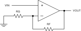
 Figure 10-1 Schematic Representation
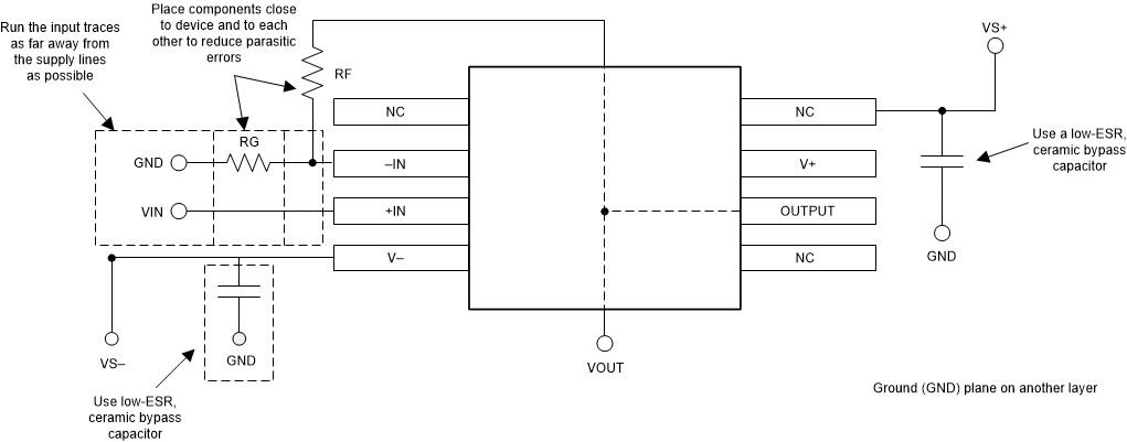
 Figure 10-2 Operational Amplifier Board Layout for Noninverting Configuration
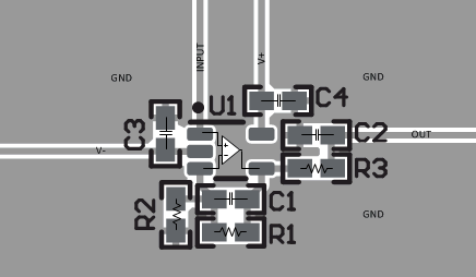
 Figure 10-3 Example Layout for SC70 (DCK) Package
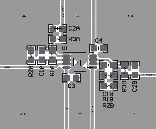
 Figure 10-4 Example Layout for VSSOP-8 (DGK) Package
 Figure 10-5 Example Layout for WSON-8 (DSG) Package