SBOSA12H March   2020  – March 2024 OPA2991-Q1 , OPA4991-Q1 , OPA991-Q1

PRODUCTION DATA  

  1.   1
  2. Features
  3. Applications
  4. Description
  5. Pin Configuration and Functions
  6. Specifications
    1. 5.1 Absolute Maximum Ratings
    2. 5.2 ESD Ratings
    3. 5.3 Recommended Operating Conditions
    4. 5.4 Thermal Information for Single Channel
    5. 5.5 Thermal Information for Dual Channel
    6. 5.6 Thermal Information for Quad Channel
    7. 5.7 Electrical Characteristics
    8. 5.8 Typical Characteristics
  7. Detailed Description
    1. 6.1 Overview
    2. 6.2 Functional Block Diagram
    3. 6.3 Feature Description
      1. 6.3.1  Input Protection Circuitry
      2. 6.3.2  EMI Rejection
      3. 6.3.3  Thermal Protection
      4. 6.3.4  Capacitive Load and Stability
      5. 6.3.5  Common-Mode Voltage Range
      6. 6.3.6  Phase Reversal Protection
      7. 6.3.7  Electrical Overstress
      8. 6.3.8  Overload Recovery
      9. 6.3.9  Typical Specifications and Distributions
      10. 6.3.10 Shutdown
    4. 6.4 Device Functional Modes
  8. Application and Implementation
    1. 7.1 Application Information
    2. 7.2 Typical Applications
      1. 7.2.1 Low-Side Current Measurement
        1. 7.2.1.1 Design Requirements
        2. 7.2.1.2 Detailed Design Procedure
        3. 7.2.1.3 Application Curve
    3. 7.3 Power Supply Recommendations
    4. 7.4 Layout
      1. 7.4.1 Layout Guidelines
      2. 7.4.2 Layout Example
  9. Device and Documentation Support
    1. 8.1 Device Support
      1. 8.1.1 Development Support
        1. 8.1.1.1 TINA-TI (Free Software Download)
        2. 8.1.1.2 TI Precision Designs
    2. 8.2 Documentation Support
      1. 8.2.1 Related Documentation
    3. 8.3 Receiving Notification of Documentation Updates
    4. 8.4 Support Resources
    5. 8.5 Trademarks
    6. 8.6 Electrostatic Discharge Caution
    7. 8.7 Glossary
  10. Revision History
  11. 10Mechanical, Packaging, and Orderable Information

Package Options

Mechanical Data (Package|Pins)
Thermal pad, mechanical data (Package|Pins)
Orderable Information

Phase Reversal Protection

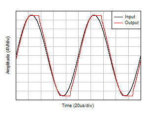
The OPAx991-Q1 family has internal phase-reversal protection. Many op amps exhibit phase reversal when the input is driven beyond its linear common-mode range. This condition is most often encountered in non-inverting circuits when the input is driven beyond the specified common-mode voltage range, causing the output to reverse into the opposite rail. The OPAx991-Q1 is a rail-to-rail input op amp; therefore, the common-mode range can extend beyond the rails. Input signals beyond the rails do not cause phase reversal; instead, the output limits into the appropriate rail. This performance is shown in Figure 6-9. For more information on phase reversal, see Op Amps With Complementary-Pair Input Stages application note.
GUID-9675E664-2CFD-478E-847C-703D2CEA0392-low.gifFigure 6-9 No Phase Reversal