SBOSA93D May   2023  – December 2024 OPT4001-Q1

PRODUCTION DATA  

  1.   1
  2. Features
  3. Applications
  4. Description
  5. Pin Configuration and Functions
  6. Specifications
    1. 5.1 Absolute Maximum Ratings
    2. 5.2 ESD Ratings
    3. 5.3 Recommended Operating Conditions
    4. 5.4 Thermal Information
    5. 5.5 Electrical Characteristics
    6. 5.6 Timing Requirements
    7. 5.7 Timing Diagram
    8. 5.8 Typical Characteristics
  7. Detailed Description
    1. 6.1 Overview
    2. 6.2 Functional Block Diagram
    3. 6.3 Feature Description
      1. 6.3.1 Spectral Matching to Human Eye
      2. 6.3.2 Automatic Full-Scale Range Setting
      3. 6.3.3 Error Correction Code (ECC) Features
        1. 6.3.3.1 Output Sample Counter
        2. 6.3.3.2 Output CRC
      4. 6.3.4 Output Register FIFO
      5. 6.3.5 Threshold Detection
    4. 6.4 Device Functional Modes
      1. 6.4.1 Modes of Operation
      2. 6.4.2 Interrupt Modes of Operation
      3. 6.4.3 Light Range Selection
      4. 6.4.4 Selecting Conversion Time
      5. 6.4.5 Light Measurement in Lux
      6. 6.4.6 Threshold Detection Calculations
      7. 6.4.7 Light Resolution
    5. 6.5 Programming
      1. 6.5.1 I2C Bus Overview
        1. 6.5.1.1 Serial Bus Address
        2. 6.5.1.2 Serial Interface
      2. 6.5.2 Writing and Reading
        1. 6.5.2.1 High-Speed I2C Mode
        2. 6.5.2.2 Burst Read Mode
        3. 6.5.2.3 General-Call Reset Command
        4. 6.5.2.4 SMBus Alert Response
  8. Register Maps
    1. 7.1 Register Descriptions
  9. Application and Implementation
    1. 8.1 Application Information
    2. 8.2 Typical Application
      1. 8.2.1 Electrical Interface
        1. 8.2.1.1 Design Requirements
          1. 8.2.1.1.1 Optical Interface
        2. 8.2.1.2 Detailed Design Procedure
          1. 8.2.1.2.1 Optomechanical Design (PicoStar Variant)
          2. 8.2.1.2.2 Optomechanical Design (USON, SOT-5X3 Variant)
        3. 8.2.1.3 Application Curves (PicoStar Variant)
        4. 8.2.1.4 Application Curves (Other Variants)
    3. 8.3 Best Design Practices
    4. 8.4 Power Supply Recommendations
    5. 8.5 Layout
      1. 8.5.1 Layout Guidelines
        1. 8.5.1.1 Soldering and Handling Recommendations (PicoStar Variant)
          1. 8.5.1.1.1 Solder Paste
          2. 8.5.1.1.2 Package Placement
          3. 8.5.1.1.3 Reflow Profile
          4. 8.5.1.1.4 Special Flexible Printed-Circuit Board (FPCB) Recommendations
          5. 8.5.1.1.5 Rework Process
        2. 8.5.1.2 Soldering and Handling Recommendations (USON, SOT-5X3 Variant)
      2. 8.5.2 Layout Example
  10. Device and Documentation Support
    1. 9.1 Documentation Support
      1. 9.1.1 Related Documentation
    2. 9.2 Receiving Notification of Documentation Updates
    3. 9.3 Support Resources
    4. 9.4 Trademarks
    5. 9.5 Electrostatic Discharge Caution
    6. 9.6 Glossary
  11. 10Revision History
  12. 11Mechanical, Packaging, and Orderable Information

Package Options

Mechanical Data (Package|Pins)
Thermal pad, mechanical data (Package|Pins)
Reflow Profile

Use the profile in Figure 8-12, and adjust if necessary. Use a slow solder reflow ramp rate of 1°C to 1.2°C/s to minimize chances of solder splattering onto the sensing area.
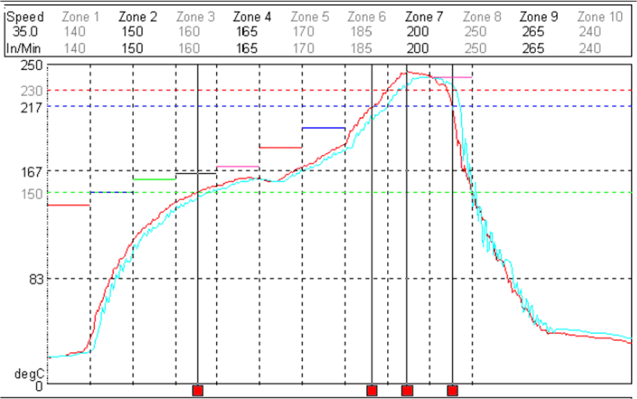
OPT4001-Q1 Recommended Solder Reflow
                    Temperature ProfileFigure 8-12 Recommended Solder Reflow Temperature Profile