SBOSA93C May 2023 – June 2024 OPT4001-Q1
PRODUCTION DATA
- 1
- 1 Features
- 2 Applications
- 3 Description
- 4 Pin Configuration and Functions
- 5 Specifications
- 6 Detailed Description
- 7 Register Maps
-
8 Application and Implementation
- 8.1 Application Information
- 8.2 Typical Application
- 8.3 Best Design Practices
- 8.4 Power Supply Recommendations
- 8.5 Layout
- 9 Device and Documentation Support
- 10Revision History
- 11Mechanical, Packaging, and Orderable Information
Package Options
Refer to the PDF data sheet for device specific package drawings
Mechanical Data (Package|Pins)
- DNP|6
- YMN|4
Thermal pad, mechanical data (Package|Pins)
Orderable Information
8.5.1.2 Soldering and Handling Recommendations (USON Variant)
The OPT4001-Q1 is qualified for three soldering reflow operations as per JEDEC JSTD-020.
Excessive heat can discolor the device and affect optical performance.
See the QFN and SON PCB Attachment application note for details on the soldering thermal profile and other information. Discard the device and do not reattach if the OPT4001-Q1 must be removed from a PCB.
As with most optical devices, take special care to make sure that optical surfaces of the device stay clean and free from damage. See Section 8.3 for more detailed recommendations. For best optical performance, solder flux and any other possible debris must be cleaned after the soldering processes.
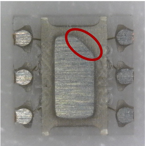
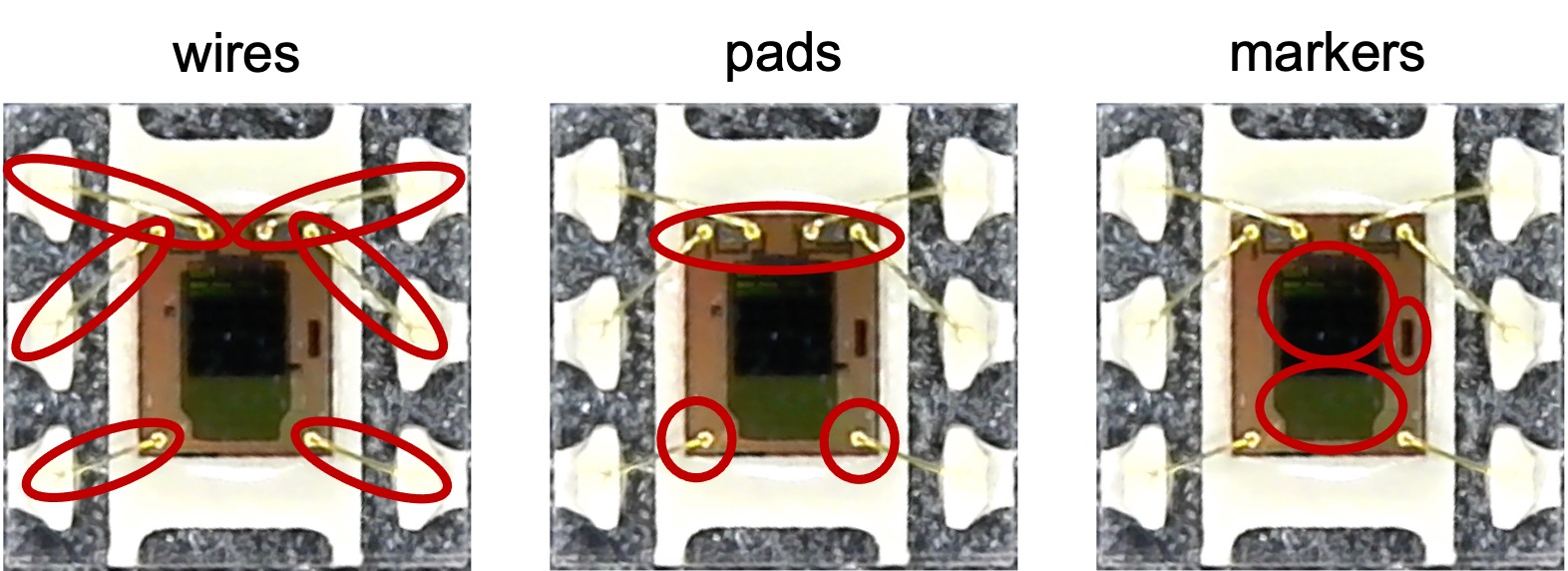
Figure 8-12 shows how to identify pin 1 on the bottom side of the package. Figure 8-13 shows various identification features for pin 1 on the top side of the package.

| NOTE: The bottom side of the device features an angled feature to denote pin 1. |
 Figure 8-13 Identification Features for Pin 1 on the Package