SBASA69B
August 2023 – December 2024
OPT4003-Q1
PRODUCTION DATA
1
1
Features
2
Applications
3
Description
4
Pin Configuration and Functions
5
Specifications
5.1
Absolute Maximum Ratings
5.2
ESD Ratings
5.3
Recommended Operating Conditions
5.4
Thermal Information
5.5
Electrical Characteristics
5.6
Timing Requirements
5.7
Timing Diagram
5.8
Typical Characteristics
6
Detailed Description
6.1
Overview
6.2
Functional Block Diagram
6.3
Feature Description
6.3.1
Spectral Response
6.3.1.1
Channel 0: Human Eye Matching
6.3.1.2
Channel 1: Near Infrared
6.3.2
Automatic Full-Scale Range Setting
6.3.3
Error Correction Code (ECC) Features
6.3.3.1
Output Sample Counter
6.3.3.2
Output CRC
6.3.3.3
Threshold Detection
6.4
Device Functional Modes
6.4.1
Modes of Operation
6.4.2
Interrupt Modes of Operation
6.4.3
Light Range Selection
6.4.4
Selecting Conversion Time
6.4.5
Light Measurement in Lux
6.4.6
Threshold Detection Calculations
6.4.7
Light Resolution
6.5
Programming
6.5.1
I2C Bus Overview
6.5.1.1
Serial Bus Address
6.5.1.2
Serial Interface
6.5.2
Writing and Reading
6.5.2.1
High-Speed I2C Mode
6.5.2.2
Burst Read Mode
6.5.2.3
General-Call Reset Command
6.5.2.4
SMBus Alert Response
7
Register Maps
7.1
Register Descriptions
8
Application and Implementation
8.1
Application Information
8.2
Typical Application
8.2.1
Electrical Interface
8.2.1.1
Design Requirements
8.2.1.1.1
Optical Interface
8.2.1.2
Detailed Design Procedure
8.2.1.2.1
Optomechanical Design (USON, SOT-5X3 Variant)
8.2.1.3
Application Curves
8.3
Best Design Practices
8.4
Power Supply Recommendations
8.5
Layout
8.5.1
Layout Guidelines
8.5.1.1
Soldering and Handling Recommendations (USON, SOT-5X3 Variant)
8.5.2
Layout Example
9
Device and Documentation Support
9.1
Documentation Support
9.1.1
Related Documentation
9.2
Receiving Notification of Documentation Updates
9.3
Support Resources
9.4
Trademarks
9.5
Electrostatic Discharge Caution
9.6
Glossary
10
Revision History
11
Mechanical, Packaging, and Orderable Information
Package Options
Mechanical Data (Package|Pins)
DNP|6
MPDS564B
Thermal pad, mechanical data (Package|Pins)
Orderable Information
sbasa69b_oa
sbasa69b_pm
8.5.2
Layout Example
Figure 8-8
Layout Example for DTS Package
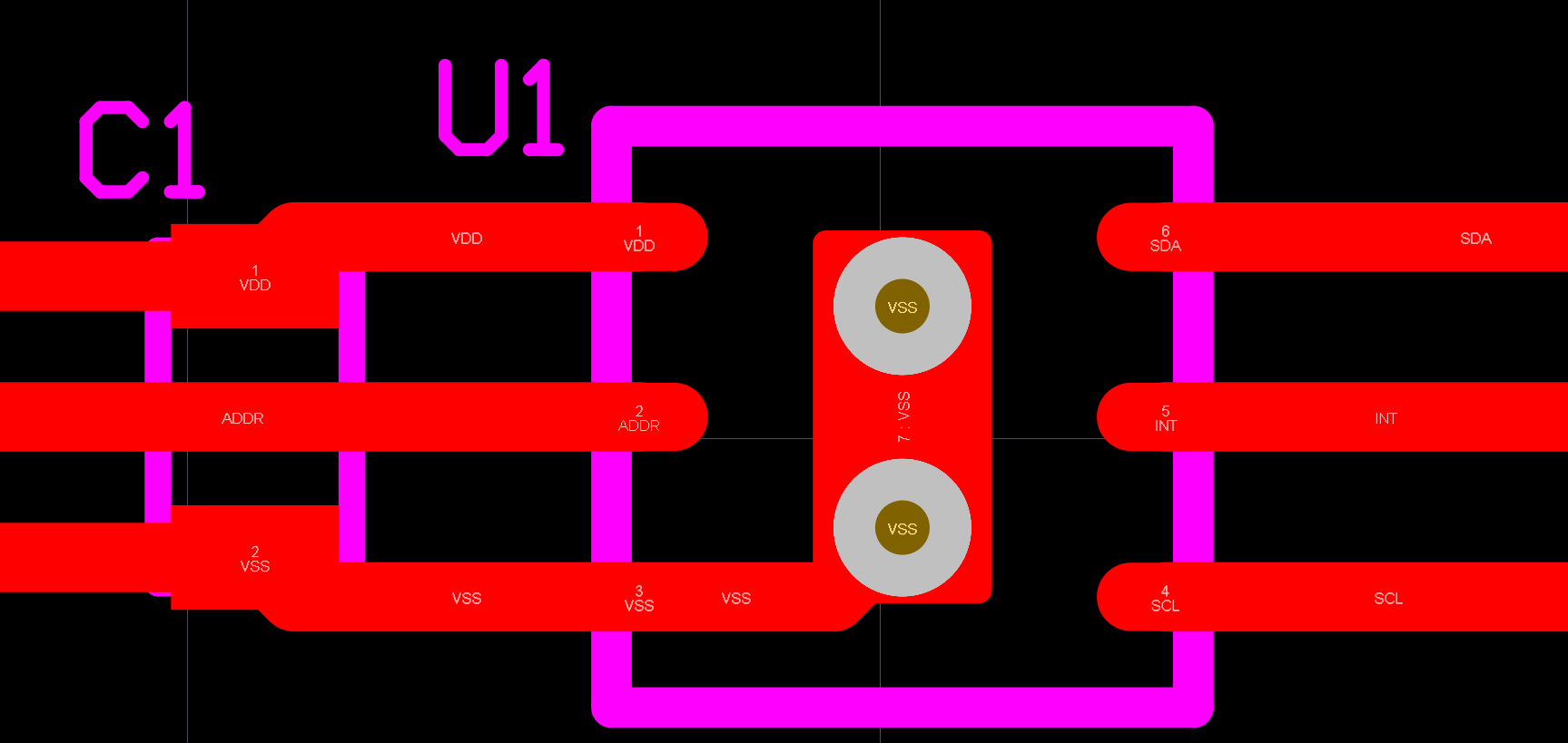
Figure 8-9
Layout Example for DNP Package