SCPS232B March 2012 – March 2016 PCA9515B
PRODUCTION DATA.
- 1 Features
- 2 Applications
- 3 Description
- 4 Revision History
- 5 Pin Configuration and Functions
- 6 Specifications
- 7 Parameter Measurement Information
- 8 Detailed Description
- 9 Application and Implementation
- 10Power Supply Recommendations
- 11Layout
- 12Device and Documentation Support
- 13Mechanical, Packaging, and Orderable Information
Package Options
Mechanical Data (Package|Pins)
- DGK|8
Thermal pad, mechanical data (Package|Pins)
Orderable Information
9 Application and Implementation
NOTE
Information in the following applications sections is not part of the TI component specification, and TI does not warrant its accuracy or completeness. TI’s customers are responsible for determining suitability of components for their purposes. Customers should validate and test their design implementation to confirm system functionality.
9.1 Application Information
The PCA9515B is typically used to buffer an I2C signal, isolating capacitance from two sides of the bus. This allows for longer traces and cables, and a more robust I2C communication. Typical Application section describes how the PCA9515B may be used to isolate a standard mode and fast mode I2C bus, to allow for faster communications when required, but maintaining compatibility with the slower standard mode slave device.
It is critical to keep the VOL and VIL requirements in mind when designing with buffers, especially when using multiple buffers/translators on the same node. Care must be taken to not violate the VIL requirement of a buffer, otherwise I2C communication errors will occur. An example of this would be a buffer with a VOL of ~0.5 V, and a device requires a VIL of less than 0.4 V. Such a connection would result in the slave device being unable to recognize the output low signal as a valid low.
9.2 Typical Application
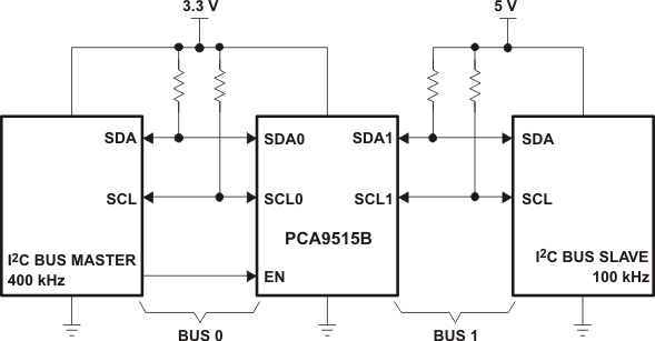
A typical application is shown in Figure 5. In this example, the system master is running on a 3.3 V I2C bus, while the slave is connected to a 5-V bus. Both buses run at 100 kHz, unless the slave bus is isolated. If the slave bus is isolated (by pulling the EN pin low), the master bus can run at 400 kHz. Master devices can be placed on either bus, the PCA9515B does not care which side the master is on. Decoupling capacitors are required, but are not shown in Figure 5 for simplicity.
 Figure 5. Typical Application
9.2.1 Design Requirements
Table 2 lists the design requirements.
Table 2. Design Requirements
| PARAMETER | VALUE |
|---|---|
| Input-side I2C signal | 3.3 V |
| Output-side I2C signal | 5 V |
9.2.2 Detailed Design Procedure
The PCA9515B is 5.5 V tolerant, so it does not require any additional circuitry to translate between the different bus voltages. When one side of the PCA9515B is pulled low by a device on the I2C bus, a CMOS hysteresis-type input detects the falling edge and causes an internal driver on the other side to turn on, thus causing the other side also to go low. The side driven low by the PCA9515B typically is at VOL = 0.5 V.
Figure 6 and Figure 7 show the waveforms that are seen in a typical application. If the bus master in Figure 5 writes to the slave through the PCA9515B, Bus 0 has the waveform shown in Figure 6. The waveform looks like a normal I2C transmission until the falling edge of the eighth clock pulse. At that point, the master releases the data line (SDA) while the slave pulls it low through the PCA9515B. Because the VOL of the PCA9515B typically is around 0.5 V, a step in the SDA is seen. After the master has transmitted the ninth clock pulse, the slave releases the data line.
On the Bus 1 side of the PCA9515B, the clock and data lines have a positive offset from ground equal to the VOL of the PCA9515B. After the eighth clock pulse, the data line is pulled to the VOL of the slave device, which is very close to ground in the example.
9.2.3 Application Curves
 Figure 6. Bus 0 Waveforms
 Figure 7. Bus 1 Waveforms