SCPS130H
August 2005 – March 2021
PCA9539
PRODUCTION DATA
1
Features
2
Description
3
Revision History
4
Description (Continued)
5
Pin Configuration and Functions
6
Specifications
6.1
Absolute Maximum Ratings
6.2
ESD Ratings
6.3
Recommended Operating Conditions
6.4
Thermal Resistance Characteristics
6.5
Electrical Characteristics
6.6
I2C Interface Timing Requirements
6.7
RESET Timing Requirements
6.8
Switching Characteristics
6.9
Typical Characteristics
7
Parameter Measurement Information
8
Detailed Description
8.1
Functional Block Diagram
8.2
Device Functional Modes
8.2.1
RESET Input
8.2.1.1
RESET Errata
8.2.1.1.1
System Impact
8.2.1.1.2
System Workaround
8.2.2
Power-On Reset
8.2.3
I/O Port
8.2.4
Interrupt ( INT) Output
8.2.4.1
Interrupt Errata
8.2.4.1.1
System Impact
8.2.4.1.2
System Workaround
8.3
Programming
8.3.1
I2C Interface
8.3.2
Register Map
8.3.2.1
Device Address
8.3.2.2
Control Register And Command Byte
8.3.2.3
Register Descriptions
8.3.2.4
Bus Transactions
8.3.2.4.1
Writes
8.3.2.4.2
Reads
9
Application Information Disclaimer
9.1
Application Information
9.2
Typical Application
9.2.1
Detailed Design Procedure
9.2.1.1
Minimizing ICC When I/O Is Used To Control Led
10
Power Supply Recommendations
10.1
Power-On Reset Requirements
11
Device and Documentation Support
11.1
Trademarks
11.2
Electrostatic Discharge Caution
11.3
Glossary
12
Mechanical, Packaging, and Orderable Information
Package Options
Mechanical Data (Package|Pins)
DGV|24
MPDS006C
PW|24
MPDS363A
DBQ|24
MPDS211A
RGE|24
MPQF124G
DW|24
MPDS174A
DB|24
MPDS509
Thermal pad, mechanical data (Package|Pins)
RGE|24
QFND008AA
Orderable Information
scps130h_oa
scps130h_pm
9.2
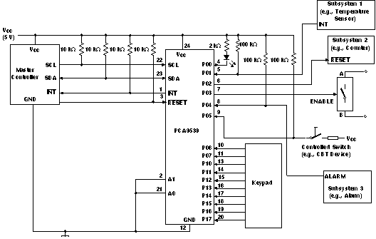
Typical Application
Device address is configured as 1110100 for this example.
P00, P02, and P03 are configured as outputs.
P01 and P04 to P17 are configured as inputs.
Pin numbers shown are for DB, DBQ, DGV, DW, and PW packages.
Figure 9-1
Typical Application