SCPS147E October 2005 – March 2021 PCA9545A
PRODUCTION DATA
- 1 Features
- 2 Applications
- 3 Description
- 4 Revision History
- 5 Pin Configuration and Functions
- 6 Specifications
- 7 Parameter Measurement Information
- 8 Detailed Description
- 9 Application Information Disclaimer
- 10Power Supply Recommendations
- 11Layout
- 12Device and Documentation Support
- 13Mechanical, Packaging, and Orderable Information
Package Options
Mechanical Data (Package|Pins)
Thermal pad, mechanical data (Package|Pins)
Orderable Information
5 Pin Configuration and Functions
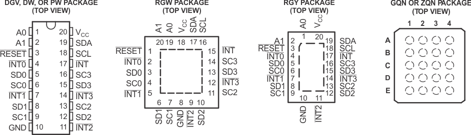
Table 5-1 Pin Functions
| PIN | DESCRIPTION | |||
|---|---|---|---|---|
| NAME | DGV, DW, PW, AND RGY |
RGW | GQN AND ZQN | |
| A0 | 1 | 19 | A2 | Address input 0. Connect directly to VCC or ground. |
| A1 | 2 | 20 | A1 | Address input 1. Connect directly to VCC or ground. |
| RESET | 3 | 1 | B3 | Active-low reset input. Connect to VDPUM(1) through a pull-up resistor, if not used. |
| INT0 | 4 | 2 | B1 | Active-low interrupt input 0. Connect to VDPU0(1) through a pull-up resistor. |
| SD0 | 5 | 3 | C2 | Serial data 0. Connect to VDPU0(1) through a pull-up resistor. |
| SC0 | 6 | 4 | C1 | Serial clock 0. Connect to VDPU0(1)through a pull-up resistor. |
| INT1 | 7 | 5 | D3 | Active-low interrupt input 1. Connect to VDPU1(1) through a pull-up resistor. |
| SD1 | 8 | 6 | D1 | Serial data 1. Connect to VDPU1(1) through a pull-up resistor. |
| SC1 | 9 | 7 | E2 | Serial clock 1. Connect to VDPU1(1) through a pull-up resistor. |
| GND | 10 | 8 | E1 | Ground |
| INT2 | 11 | 9 | E3 | Active-low interrupt input 2. Connect to VDPU2(1) through a pull-up resistor. |
| SD2 | 12 | 10 | E4 | Serial data 2. Connect to VDPU2(1) through a pull-up resistor. |
| SC2 | 13 | 11 | D2 | Serial clock 2. Connect to VDPU2(1) through a pull-up resistor. |
| INT3 | 14 | 12 | D4 | Active-low interrupt input 3. Connect to VDPU3(1) through a pull-up resistor. |
| SD3 | 15 | 13 | C3 | Serial data 3. Connect to VDPU3(1) through a pull-up resistor. |
| SC3 | 16 | 14 | C4 | Serial clock 3. Connect to VDPU3(1) through a pull-up resistor. |
| INT | 17 | 15 | B2 | Active-low interrupt output. Connect to VDPUM(1) through a pull-up resistor. |
| SCL | 18 | 16 | B4 | Serial clock line. Connect to VDPUM(1) through a pull-up resistor. |
| SDA | 19 | 17 | A4 | Serial data line. Connect to VDPUM(1) through a pull-up resistor. |
| VCC | 20 | 18 | A3 | Supply power |
(1) VDPUX is the pull-up reference voltage for the
associated data line. VDPUM is the master I2C reference
voltage while VDPU0-VDPU3 are the slave channel reference
voltages.