SCPS148I
October 2005 – June 2022
PCA9546A
PRODUCTION DATA
1
Features
2
Applications
3
Description
4
Revision History
5
Pin Configuration and Functions
6
Specifications
6.1
Absolute Maximum Ratings
6.2
ESD Ratings
6.3
Recommended Operating Conditions
6.4
Thermal Information
6.5
Electrical Characteristics
6.6
I2C Interface Timing Requirements
6.7
Interrupt and Reset Timing Requirements
6.8
Switching Characteristics
7
Parameter Measurement Information
16
8
Detailed Description
8.1
Overview
8.2
Functional Block Diagram
8.3
Feature Description
8.4
Device Functional Modes
8.4.1
RESET Input
8.4.1.1
RESET Errata
24
25
8.4.2
Power-On Reset
8.5
Programming
8.5.1
I2C Interface
8.6
Control Register
8.6.1
Device Address
8.6.2
Control Register Description
8.6.3
Control Register Definition
9
Application Information Disclaimer
9.1
Application Information
9.2
Typical Application
9.2.1
Design Requirements
9.2.2
Detailed Design Procedure
9.2.3
Application Curves
10
Power Supply Recommendations
10.1
Power-On Reset Requirements
11
Layout
11.1
Layout Guidelines
11.2
Layout Example
12
Device and Documentation Support
12.1
Receiving Notification of Documentation Updates
12.2
Support Resources
12.3
Trademarks
12.4
Electrostatic Discharge Caution
12.5
Glossary
13
Mechanical, Packaging, and Orderable Information
Package Options
Mechanical Data (Package|Pins)
DGV|16
MPDS006C
DW|16
MSOI003I
PW|16
MPDS361A
RGY|16
MPQF115G
D|16
MPDS178G
RGV|16
MPQF121F
Thermal pad, mechanical data (Package|Pins)
DW|16
QFND313D
RGY|16
QFND040P
RGV|16
QFND107G
Orderable Information
scps148i_oa
scps148i_pm
9.2.3
Application Curves
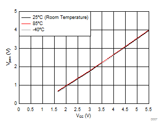
Figure 9-2
Pass-Gate Voltage (V
pass
) vs Supply Voltage (V
CC
) at Three Temperature Points
V
OL
= 0.2*V
DPUX
, I
OL
= 2 mA when V
DPUX
≤ 2 V
V
OL
= 0.4 V, I
OL
= 3 mA when V
DPUX
> 2 V
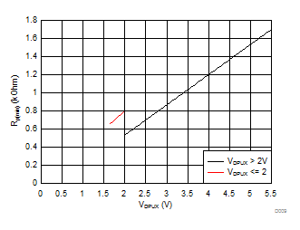
Figure 9-4
Minimum Pull-Up Resistance (R
p(min)
) vs Pull-Up Reference Voltage (V
DPUX
)
Standard-mode (f
SCL
= 100 kHz, t
r
= 1 µs)
Fast-mode (f
SCL
= 400 kHz, t
r
= 300 ns)
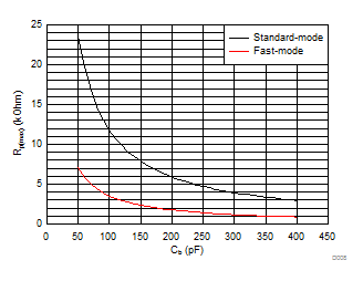
Figure 9-3
Maximum Pull-Up resistance (R
p(max)
) vs Bus Capacitance (C
b
)