SCPS128D July   2006  – March 2021 PCA9554

PRODUCTION DATA  

  1. Features
  2. Description
  3. Revision History
  4. Description (Continued)
  5. Pin Configuration and Functions
  6. Specifications
    1. 6.1 Absolute Maximum Ratings
    2. 6.2 ESD Ratings
    3. 6.3 Recommended Operating Conditions
    4. 6.4 Thermal Information
    5. 6.5 Electrical Characteristics
    6. 6.6 I2C Interface Timing Requirements
    7. 6.7 Switching Characteristics
    8. 6.8 Typical Characteristics
  7. Parameter Measurement Information
  8. Detailed Description
    1. 8.1 Functional Block Diagram
    2. 8.2 Device Functional Modes
      1. 8.2.1 Power-On Reset
      2. 8.2.2 I/O Port
      3. 8.2.3 Interrupt Output ( INT)
        1. 8.2.3.1 Interrupt Errata
          1.        23
          2. 8.2.3.1.1 24
          3. 8.2.3.1.2 25
    3. 8.3 Programming
      1. 8.3.1 I2C Interface
      2. 8.3.2 Register Map
        1. 8.3.2.1 Device Address
        2. 8.3.2.2 Control Register And Command Byte
        3. 8.3.2.3 Register Descriptions
        4. 8.3.2.4 Bus Transactions
          1. 8.3.2.4.1 Writes
          2. 8.3.2.4.2 Reads
  9. Application Information Disclaimer
    1. 9.1 Application Information
      1. 9.1.1 Typical Application
        1. 9.1.1.1 Design Requirements
          1. 9.1.1.1.1 Minimizing ICC When I/Os Control Leds
  10. 10Power Supply Recommendations
    1. 10.1 Power-On Reset Requirements
  11. 11Device and Documentation Support
    1. 11.1 Receiving Notification of Documentation Updates
    2. 11.2 Support Resources
    3. 11.3 Trademarks
    4. 11.4 Electrostatic Discharge Caution
    5. 11.5 Glossary
  12. 12Mechanical, Packaging, and Orderable Information

Package Options

Mechanical Data (Package|Pins)
Thermal pad, mechanical data (Package|Pins)
Orderable Information

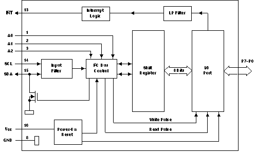
Functional Block Diagram

GUID-37A46927-A501-45CD-8194-0DE7FACCD342-low.gif
Pin numbers shown are for the DB, DBQ, DGV, DW, N, or PW package.
All I/Os are set to inputs at reset.
Figure 8-1 Logic Diagram
GUID-434F48E4-6413-48C7-8097-1B39CD6FEB78-low.gif
At power-on reset, all registers return to default values.
Figure 8-2 Simplified Schematic Of P0 To P7