SCPS068K July 2001 – September 2024 PCF8574
PRODUCTION DATA
- 1
- 1 Features
- 2 Applications
- 3 Description
- 4 Pin Configuration and Functions
- 5 Specifications
- 6 Parameter Measurement Information
- 7 Detailed Description
- 8 Application and Implementation
- 9 Device and Documentation Support
- 10Revision History
- 11Mechanical, Packaging, and Orderable Information
8.2.1.1 Minimizing ICC When I/Os Control LEDs
When the I/Os are used to control LEDs, normally they are connected to VCC through a resistor as shown in Figure 8-1. For a P-port configured as an input, ICC increases as VI becomes lower than VCC. The LED is a diode, with threshold voltage VT, and when a P-port is configured as an input the LED will be off but VI is a VT drop below VCC.
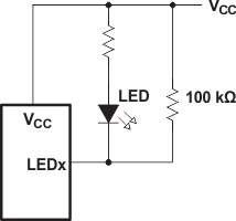
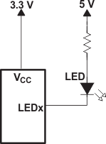
For battery-powered applications, it is essential that the voltage of P-ports controlling LEDs is greater than or equal to VCC when the P-ports are configured as input to minimize current consumption. Figure 8-2 shows a high-value resistor in parallel with the LED. Figure 8-3 shows VCC less than the LED supply voltage by at least VT. Both of these methods maintain the I/O VI at or above VCC and prevents additional supply current consumption when the P-port is configured as an input and the LED is off.
 Figure 8-2 High-Value Resistor in Parallel With LED
 Figure 8-3 Device Supplied by a Lower Voltage