SCPS069H July   2001  – September 2024 PCF8574A

PRODUCTION DATA  

  1.   1
  2. Features
  3. Applications
  4. Description
  5. Pin Configuration and Functions
  6. Specifications
    1. 5.1 Absolute Maximum Ratings
    2. 5.2 ESD Ratings
    3. 5.3 Recommended Operating Conditions
    4. 5.4 Thermal Information
    5. 5.5 Electrical Characteristics
    6. 5.6 I2C Interface Timing Requirements
    7. 5.7 Switching Characteristics
    8. 5.8 Typical Characteristics
  7. Parameter Measurement Information
  8. Detailed Description
    1. 7.1 Overview
    2. 7.2 Functional Block Diagram
      1. 7.2.1 Simplified Block Diagram of Device
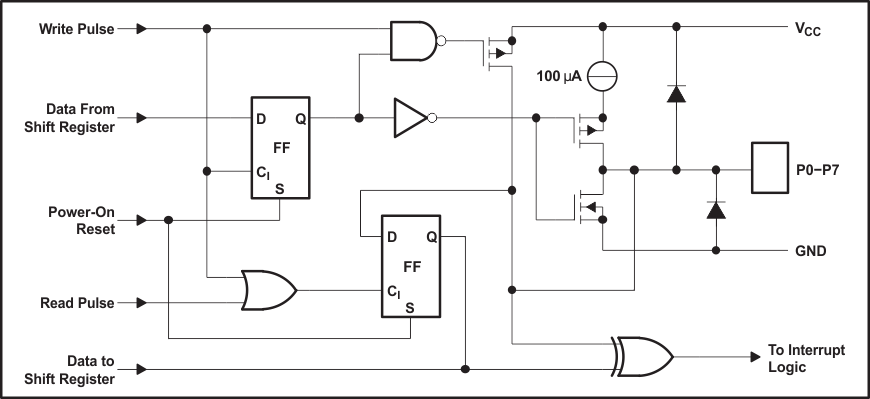
      2. 7.2.2 Simplified Schematic Diagram of Each P-Port Input/Output
    3. 7.3 Feature Description
      1. 7.3.1 I2C Interface
      2. 7.3.2 Interface Definition
      3. 7.3.3 Address Reference
    4. 7.4 Device Functional Modes
  9. Application Information Disclaimer
    1. 8.1 Application Information
    2. 8.2 Typical Application
      1. 8.2.1 Design Requirements
        1. 8.2.1.1 Minimizing ICC When I/Os Control LEDs
      2. 8.2.2 Detailed Design Procedure
      3. 8.2.3 Application Curves
    3. 8.3 Power Supply Recommendations
      1. 8.3.1 Power-On Reset Requirements
    4. 8.4 Layout
      1. 8.4.1 Layout Guidelines
      2. 8.4.2 Layout Example
  10. Device and Documentation Support
    1. 9.1 Documentation Support
      1. 9.1.1 Glossary
    2. 9.2 Receiving Notification of Documentation Updates
    3. 9.3 Support Resources
    4. 9.4 Trademarks
    5. 9.5 Electrostatic Discharge Caution
    6. 9.6 Glossary
  11. 10Revision History
  12. 11Mechanical, Packaging, and Orderable Information

Package Options

Refer to the PDF data sheet for device specific package drawings

Mechanical Data (Package|Pins)
  • DGV|20
  • DW|16
  • N|16
  • PW|20
  • RGY|20
Thermal pad, mechanical data (Package|Pins)
Orderable Information

Simplified Schematic Diagram of Each P-Port Input/Output

PCF8574A