SCPS121I January   2005  – August 2024 PCF8575

PRODUCTION DATA  

  1.   1
  2. Features
  3. Applications
  4. Description
  5. Pin Configuration and Functions
  6. Specifications
    1. 5.1 Absolute Maximum Ratings
    2. 5.2 ESD Ratings
    3. 5.3 Recommended Operating Conditions
    4. 5.4 Thermal Information
    5. 5.5 Electrical Characteristics
    6. 5.6 I2C Interface Timing Requirements
    7. 5.7 Switching Characteristics
  7. Typical Characteristics
  8. Parameter Measurement Information
  9. Detailed Description
    1. 8.1 Overview
    2. 8.2 Functional Block Diagram
    3. 8.3 Feature Description
      1. 8.3.1 I2C Interface
      2. 8.3.2 Interface Definition
      3. 8.3.3 Address Reference
    4. 8.4 Device Functional Modes
  10. Application and Implementation
    1. 9.1 Application Information
    2. 9.2 Typical Application
      1. 9.2.1 Design Requirements
        1. 9.2.1.1 Minimizing ICC When I/Os Control LEDs
      2. 9.2.2 Detailed Design Procedure
      3. 9.2.3 Application Curves
    3. 9.3 Power Supply Recommendations
      1. 9.3.1 Power-On Reset
      2. 9.3.2 System Impact
    4. 9.4 Layout
      1. 9.4.1 Layout Guidelines
      2. 9.4.2 Layout Example
  11. 10Device and Documentation Support
    1. 10.1 Device Support
    2. 10.2 Documentation Support
    3. 10.3 Receiving Notification of Documentation Updates
    4. 10.4 Support Resources
    5. 10.5 Trademarks
    6. 10.6 Electrostatic Discharge Caution
    7. 10.7 Glossary
  12. 11Revision History
  13. 12Mechanical, Packaging, and Orderable Information

Package Options

Mechanical Data (Package|Pins)
Thermal pad, mechanical data (Package|Pins)
Orderable Information

Device Functional Modes

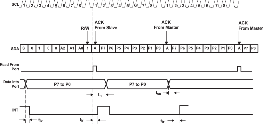
Figure 8-6 and Figure 8-7 show the address and timing diagrams for the write and read modes, respectively.
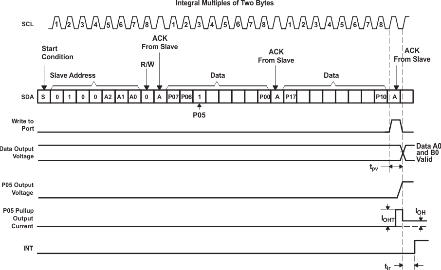
PCF8575 Write Mode (Output)Figure 8-6 Write Mode (Output)
PCF8575 Read Mode (Input)Figure 8-7 Read Mode (Input)