SLES211C February 2008 – July 2015 PCM1681 , PCM1681-Q1
PRODUCTION DATA.
- 1 Features
- 2 Applications
- 3 Description
- 4 Revision History
- 5 Description (continued)
- 6 Pin Configuration and Functions
- 7 Specifications
-
8 Detailed Description
- 8.1 Overview
- 8.2 Functional Block Diagram
- 8.3 Feature Description
- 8.4 Device Functional Modes
- 8.5 Programming
- 8.6
Register Maps
- 8.6.1 Reserved Registers
- 8.6.2
Register Definitions
- 8.6.2.1 ATx[7:0]: Digital Attenuation Level Setting
- 8.6.2.2 MUTx: Soft Mute Control
- 8.6.2.3 DACx: DAC Operation Control
- 8.6.2.4 FLT: Digital Filter Roll-Off Control
- 8.6.2.5 FMT[3:0]: Audio Interface Data Format
- 8.6.2.6 SRST: Reset
- 8.6.2.7 ZREV: Zero-Flag Polarity Select
- 8.6.2.8 DREV: Output Phase Select
- 8.6.2.9 DMF[1:0]: Sampling Frequency Selection for the De-Emphasis Function
- 8.6.2.10 DMC: Digital De-Emphasis All-Channel Function Control
- 8.6.2.11 REV[8:1]: Output Phase Select per Channel
- 8.6.2.12 OVER: Oversampling Rate Control
- 8.6.2.13 FLTx: Digital Filter Roll-Off Control per DATA Group
- 8.6.2.14 DAMS: Digital Attenuation Mode Select
- 8.6.2.15 AZRO[1:0]: Zero-Flag Channel-Combination Select
- 8.6.2.16 ZERO[8:1]: Zero-Detect Status (Read-Only, I2C Interface Only)
- 9 Application and Implementation
- 10Power Supply Recommendations
- 11Layout
- 12Device and Documentation Support
- 13Mechanical, Packaging, and Orderable Information
Package Options
Mechanical Data (Package|Pins)
- PWP|28
Thermal pad, mechanical data (Package|Pins)
- PWP|28
Orderable Information
7 Specifications
7.1 Absolute Maximum Ratings(1)
Over operating free-air temperature range (unless otherwise noted).| MIN | MAX | UNIT | ||
|---|---|---|---|---|
| Supply voltage | VCC1, VCC2 | –0.3 | 6.5 | V |
| VDD | –0.3 | 4 | V | |
| Supply voltage differences | VCC1, VCC2 | –0.1 | 0.1 | V |
| Ground voltage differences | AGND1, AGND2, DGND | –0.1 | V | |
| Input voltage to digital pins | ZR1/ZR1/FMT0, ZR2, MSEL | –0.3 | VDD + 0.3, < 4 | V |
| MS/ADR/FMT1, MC/SCL/DEMP, MD/SDA/MUTE, SCK, BCK, LRCK, DATA1, 2, 3, 4 |
–0.3 | 6.5 | V | |
| Input voltage to analog pins | –0.3 | VCC + 0.3, < 6.5 | V | |
| Input current any pins except supplies | –10 | 10 | mA | |
| Ambient temperature under bias | –40 | 125 | °C | |
| Junction temperature , TJ | 150 | °C | ||
| Package temperature (IR reflow, peak) | 260 | °C | ||
| Storage temperature, Tstg | –55 | 150 | °C | |
(1) Stresses beyond those listed under absolute maximum ratings may cause permanent damage to the device. These are stress ratings only, and functional operation of the device at these or any other conditions beyond those indicated under recommended operating conditions is not implied. Exposure to absolute-maximum-rated conditions for extended periods may affect device reliability.
7.2 ESD Ratings: PCM1681
| VALUE | UNIT | |||
|---|---|---|---|---|
| V(ESD) | Electrostatic discharge | Human body model (HBM), per ANSI/ESDA/JEDEC JS-001(1) | ±4000 | V |
| Charged-device model (CDM), per JEDEC specification JESD22-C101(2) | ±1000 | |||
(1) JEDEC document JEP155 states that 500-V HBM allows safe manufacturing with a standard ESD control process.
(2) JEDEC document JEP157 states that 250-V CDM allows safe manufacturing with a standard ESD control process.
7.3 ESD Ratings: PCM1681-Q1
| VALUE | UNIT | |||
|---|---|---|---|---|
| V(ESD) | Electrostatic discharge | Human-body model (HBM), per AEC Q100-002(1) | ±2000 | V |
| Charged-device model (CDM), per AEC Q100-011 | ±1000 | |||
(1) AEC Q100-002 indicates that HBM stressing shall be in accordance with the ANSI/ESDA/JEDEC JS-001 specification.
7.4 Recommended Operating Conditions
Over operating free-air temperature range.| MIN | NOM | MAX | UNIT | ||
|---|---|---|---|---|---|
| Analog supply voltage, VCC1, VCC2 | 4.5 | 5 | 5.5 | V | |
| Digital supply voltage, VDD | 3 | 3.3 | 3.6 | V | |
| Digital input logic family | TTL | ||||
| Digital input clock frequency | System clock | 1.024 | 36.864 | MHz | |
| Sampling clock | 8 | 192 | kHz | ||
| Analog output load resistance | 5 | kΩ | |||
| Analog output load capacitance | 50 | pF | |||
| Digital output load capacitance | 20 | pF | |||
| Operating free-air temperature, TA | PCM1681 | –40 | 85 | °C | |
| PCM1681-Q1 | –40 | 105 | °C | ||
7.5 Thermal Information
| THERMAL METRIC(1) | PCM1681, PCM1681-Q1 | UNIT | |
|---|---|---|---|
| PWP (HTSSOP) | |||
| 28 PINS | |||
| RθJA | Junction-to-ambient thermal resistance | 31 | °C/W |
| RθJC(top) | Junction-to-case (top) thermal resistance | 14.9 | °C/W |
| RθJB | Junction-to-board thermal resistance | 12.6 | °C/W |
| ψJT | Junction-to-top characterization parameter | 0.4 | °C/W |
| ψJB | Junction-to-board characterization parameter | 12.4 | °C/W |
| RθJC(bot) | Junction-to-case (bottom) thermal resistance | 1.1 | °C/W |
(1) For more information about traditional and new thermal metrics, see the Semiconductor and IC Package Thermal Metrics application report, SPRA953.
7.6 Electrical Characteristics
All specifications at VCC = 5.0 V, VDD = 3.3 V, fS = 48 kHz, system clock = 512 fS, and 24-bit data, narrow o/s mode, unless otherwise noted.| PARAMETER | TEST CONDITIONS | MIN | TYP | MAX | UNIT | |
|---|---|---|---|---|---|---|
| RESOLUTION | 24 | bits | ||||
| DATA FORMAT | ||||||
| Audio data interface format | Right-justified, I2S, left-justified, TDM | |||||
| Audio data bit length | 16-, 18-, 20-, or 24-bits, selectable | |||||
| Audio data format | MSB-first, 2s complement | |||||
| fS | Sampling frequency | 5 | 200 | kHz | ||
| System clock frequency | 128, 192, 256, 384, 512, 768, 1152 fS |
|||||
| DIGITAL INPUT/OUTPUT | ||||||
| Logic family | TTL compatible | |||||
| VIH(1) | Input logic level | 2.0 | VDD | VDC | ||
| VIL(1) | 0.8 | |||||
| VIH(2) | 2.0 | 5.5 | ||||
| VIL(2) | 0.8 | |||||
| IIH(1)(2) | Input logic current | VIN = VDD | 10 | μA | ||
| IIL(1)(2) | VIN = 0 V | –10 | ||||
| VOH(3) | Output logic level | IOH = –1 mA | 2.4 | VDC | ||
| VOL(3)(4) | IOL = 1 mA | 0.4 | ||||
| DYNAMIC PERFORMANCE(5) | ||||||
| THD+N | Total harmonic distortion + noise | VOUT = 0 dB, fS = 48 kHz | 0.002% | 0.008% | ||
| VOUT = 0 dB, fS = 96 kHz, system clock = 256 fS | 0.002% | |||||
| VOUT = 0 dB, fS = 192 kHz, system clock = 128 fS |
0.002% | |||||
| Dynamic range | EIAJ, A-weighted, fS = 48 kHz | 100 | 105 | dB | ||
| A-weighted, fS = 96 kHz, system clock = 256 fS | 105 | |||||
| A-weighted, fS = 192 kHz, system clock = 128 fS | 105 | |||||
| SNR | Signal-to-noise ratio | EIAJ, A-weighted, fS = 48 kHz | 100 | 105 | dB | |
| A-weighted, fS = 96 kHz, system clock = 256 fS | 105 | |||||
| A-weighted, fS = 192 kHz, system clock = 128 fS | 105 | |||||
| Channel separation | fS = 48 kHz | 94 | 102 | dB | ||
| fS = 96 kHz, system clock = 256 fS | 102 | |||||
| fS = 192 kHz, system clock = 128 fS | 102 | |||||
| DC ACCURACY | ||||||
| Gain error | ±2.0 | ±6 | % of FSR | |||
| Gain mismatch, channel-to-channel | ±2.0 | ±6 | % of FSR | |||
| Bipolar zero error | VOUT = 0.486 VCC at BPZ input | ±30 | ±80 | mV | ||
| ANALOG OUTPUT | ||||||
| Output voltage | Full-scale (–0 dB) | 0.75 VCC | VPP | |||
| Bipolar zero voltage | 0.486 VCC | VDC | ||||
| Load impedance | AC-coupled load | 5 | kΩ | |||
| DIGITAL FILTER PERFORMANCE | ||||||
| Filter Characteristics (Sharp Roll-Off) | ||||||
| Passband | ±0.015 dB | 0.454 fS | ||||
| Stop band | 0.546 fS | |||||
| Passband ripple | ±0.015 | dB | ||||
| Stop band attenuation | Stop band = 0.546 fS | –57 | dB | |||
| Filter Characteristics (Slow Roll-Off) | ||||||
| Passband | ±0.004 dB | 0.261 fS | ||||
| Stop band | 0.727 fS | |||||
| Passband ripple | ±0.004 | dB | ||||
| Stop band attenuation | Stop band = 0.727 fS | –56 | dB | |||
| Filter Characteristics | ||||||
| Delay time | 24/fS | |||||
| De-emphasis error | ±0.1 | dB | ||||
| ANALOG FILTER PERFORMANCE | ||||||
| Frequency response | at 20 kHz | –0.02 | dB | |||
| at 44 kHz | –0.07 | |||||
| POWER-SUPPLY REQUIREMENTS | ||||||
| VDD | Voltage range | 3 | 3.3 | 3.6 | VDC | |
| VCC | 4.5 | 5.0 | 5.5 | |||
| IDD | Supply current | fS = 48 kHz | 13 | 20 | mA | |
| fS = 96 kHz, system clock = 256 fS | 18 | |||||
| fS = 192 kHz, system clock = 128 fS | 23 | |||||
| ICC | Supply current | fS = 48 kHz | 62 | 80 | mA | |
| fS = 96 kHz, system clock = 256 fS | 62 | |||||
| fS = 192 kHz, system clock = 128 fS | 62 | |||||
| Power dissipation | fS = 48 kHz | 353 | 466 | mW | ||
| fS = 96 kHz, system clock = 256 fS | 369 | |||||
| fS = 192 kHz, system clock = 128 fS | 386 | |||||
| TEMPERATURE RANGE | ||||||
| Operating temperature | PCM1681 | –40 | 85 | °C | ||
| PCM1681-Q1 | –40 | 105 | °C | |||
| θJA | Thermal resistance | 28-pin TSSOP PowerPAD™ | 28 | °C/W | ||
(1) Pins 1, 14: ZR1/ZR1/FMT0 (input mode), MSEL
(2) Pins 2, 3, 4, 5, 6, 7, 8, 11, 12, 13: MS/ADR/FMT1, MC/SCL/DEMP, MD/SDA/MUTE (input mode), SCK, DATA1, BCK, LRCK, DATA2, DATA3, DATA4
(3) Pins 1, 28: ZR1/ZR1/FMT0 (output mode), ZR2
(4) Pin 4: MD/SDA/MUTE (output mode)
(5) Analog performance characteristics are measured using the System Two™ Cascade audio measurement system by Audio Precision™, fIN = 1 kHz, average mode, with 20-kHz LPF and 400-Hz HPF.
7.7 Interface Timing Requirements
| PARAMETER | MIN | MAX | UNIT | |
|---|---|---|---|---|
| f(SCL) | SCL clock frequency | 100 | kHz | |
| t(BUF) | Bus free time between a STOP and START condition | 4.7 | μs | |
| t(LOW) | Low period of the SCL clock | 4.7 | μs | |
| t(HI) | High period of the SCL clock | 4 | μs | |
| t(RS-SU) | Setup time for (repeated) START condition | 4.7 | μs | |
| t(S-HD)
t(RS-HD) |
Hold time for (repeated) START condition | 4 | μs | |
| t(D-SU) | Data setup time | 250 | ns | |
| t(D-HD) | Data hold time | 0 | 900 | ns |
| t(SCL-R) | Rise time of SCL signal | 20 + 0.1 CB | 1000 | ns |
| t(SCL-R1) | Rise time of SCL signal after a repeated START condition and after an acknowledge bit | 20 + 0.1 CB | 1000 | ns |
| t(SCL-F) | Fall time of SCL signal | 20 + 0.1 CB | 1000 | ns |
| t(SDA-R) | Rise time of SDA signal | 20 + 0.1 CB | 1000 | ns |
| t(SDA-F) | Fall time of SDA signal | 20 + 0.1 CB | 1000 | ns |
| t(P-SU) | Setup time for STOP condition | 4 | μs | |
| CB | Capacitive load for SDA and SCL lines | 400 | pF | |
| VNH | Noise margin at high level for each connected device (including hysteresis) | 0.2 VDD | V | |
 Figure 1. Interface Timing
7.8 Typical Characteristics
All specifications at TA = +25°C, VCC = 5 V, VDD = 3.3 V, fS = 48 kHz, system clock = 512 fS, and 24-bit data, unless otherwise noted.7.8.1 Digital Filter (De-Emphasis Off)
 Figure 2. Frequency Response (Sharp Roll-off)
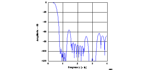 Figure 4. Frequency Response (Slow Roll-off)
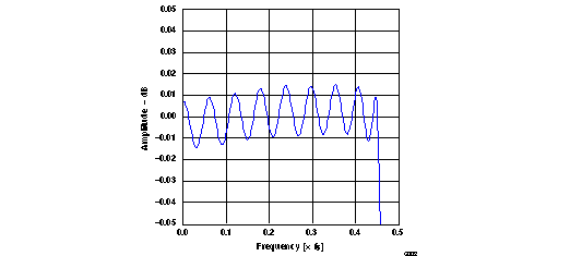 Figure 3. Passband Frequency Response (Sharp Roll-off)
 Figure 5. Transition Characteristics (Slow Roll-off)
7.8.2 De-Emphasis Filter
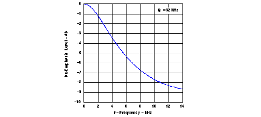 Figure 6. De-Emphasis
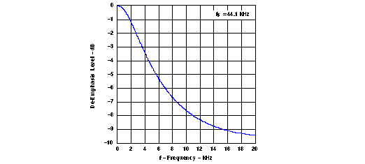 Figure 8. De-Emphasis
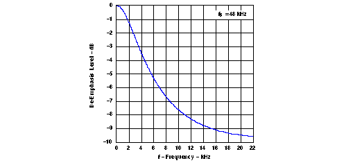 Figure 10. De-Emphasis
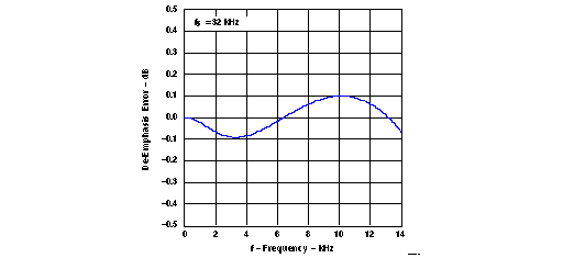 Figure 7. De-Emphasis Error
 Figure 9. De-Emphasis Error
 Figure 11. De-Emphasis Error
7.8.3 Analog Filter
 Figure 12. Analog Filter Performance
7.8.4 Analog Dynamic Performance
7.8.4.1 Supply Voltage Characteristics
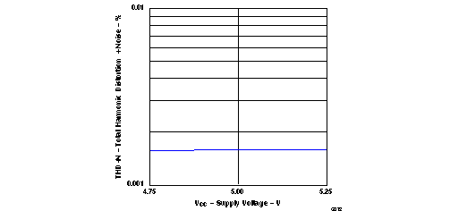 Figure 13. Total Harmonic Distortion + Noise vs Supply Voltage
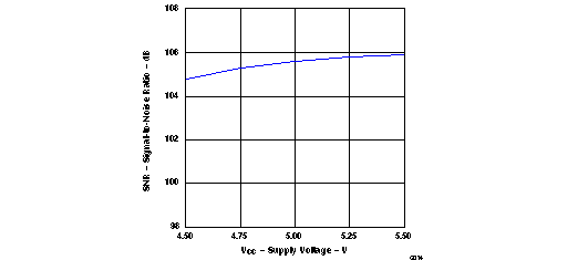 Figure 15. Signal-to-Noise Ratio vs Supply Voltage
 Figure 14. Dynamic Range vs Supply Voltage
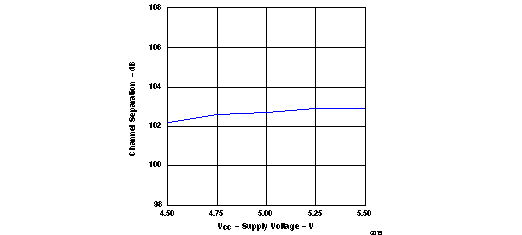 Figure 16. Channel Separation vs Supply Voltage
7.8.4.2 Temperature Characteristics
 Figure 17. Total Harmonic Distortion + Noise vs Temperature
 Figure 19. Signal-to-Noise Ratio vs Temperature
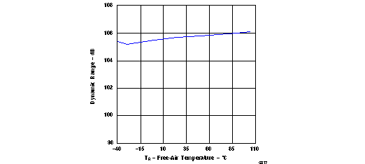 Figure 18. Dynamic Range vs Temperature
 Figure 20. Channel Separation vs Temperature