SLES254D April 2010 – July 2015 PCM1753-Q1 , PCM1754-Q1
PRODUCTION DATA.
- 1 Features
- 2 Applications
- 3 Description
- 4 Revision History
- 5 Device Comparison Table
- 6 Pin Configuration Functions
- 7 Specifications
-
8 Detailed Description
- 8.1 Overview
- 8.2 Functional Block Diagram
- 8.3 Feature Description
- 8.4 Device Functional Modes
- 8.5 Programming
- 8.6
Register Maps
- 8.6.1
Mode Control Registers (PCM1753-Q1)
- 8.6.1.1 User-Programmable Mode Controls
- 8.6.1.2
Register Definitions
- 8.6.1.2.1 ATx[7:0]: Digital Attenuation Level Setting
- 8.6.1.2.2 MUTx: Soft Mute Control
- 8.6.1.2.3 OVER: Oversampling Rate Control
- 8.6.1.2.4 SRST: Reset
- 8.6.1.2.5 DACx: DAC Operation Control
- 8.6.1.2.6 DM12: Digital De-Emphasis Function Control
- 8.6.1.2.7 DMF[1:0]: Sampling Frequency Selection for the De-Emphasis Function
- 8.6.1.2.8 FMT[2:0]: Audio Interface Data Format
- 8.6.1.2.9 FLT: Digital Filter Rolloff Control
- 8.6.1.2.10 DREV: Output Phase Select
- 8.6.1.2.11 ZREV: Zero Flag Polarity Select
- 8.6.1.2.12 AZRO: Zero Flag Function Select
- 8.6.1
Mode Control Registers (PCM1753-Q1)
- 9 Application and Implementation
- 10Power Supply Recommendations
- 11Layout
- 12Device and Documentation Support
- 13Mechanical, Packaging, and Orderable Information
Package Options
Mechanical Data (Package|Pins)
- DBQ|16
Thermal pad, mechanical data (Package|Pins)
Orderable Information
9 Application and Implementation
NOTE
Information in the following applications sections is not part of the TI component specification, and TI does not warrant its accuracy or completeness. TI’s customers are responsible for determining suitability of components for their purposes. Customers should validate and test their design implementation to confirm system functionality.
9.1 Application Information
The delta-sigma section of the PCM175x-Q1 family of devices is based on an 8-level amplitude quantizer and a 4th-order noise shaper. This section converts the oversampled input data to 8-level delta-sigma format. Figure 32 shows a block diagram of the 8-level delta-sigma modulator. This 8-level delta-sigma modulator has the advantage of stability and clock jitter sensitivity over the typical one-bit (2-level) delta-sigma modulator.
The combined oversampling rate of the delta-sigma modulator and the interpolation filter is 64 fS.
Figure 35 and Figure 36 show the theoretical quantization noise performance of the 8-level delta-sigma modulator. The enhanced multilevel delta-sigma architecture also has advantages for input clock jitter sensitivity because of the multilevel quantizer, with the simulated jitter sensitivity shown in Figure 37.
9.2 Typical Application
Figure 30 shows a basic connection diagram with the necessary power supply bypassing and decoupling components. TI recommends using the component values shown in Figure 30 for all designs.
The use of series resistors (22 Ω to 100 Ω) is recommended for the SCK, LRCK, BCK, and DATA inputs. The series resistor combines with the stray PCB and device input capacitance to form a low-pass filter, which reduces high-frequency noise emissions and helps to dampen glitches and ringing present on clock and data lines.
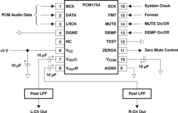 Figure 30. Basic Connection Diagram
9.2.1 Design Requirements
9.2.1.1 Power Supplies and Grounding
The PCM1754-Q1 device requires 5 V for VCC.
Proper power supply bypassing is shown in Figure 30. The 10-μF capacitors should be tantalum or aluminum electrolytic.
9.2.1.2 DAC Output Filter Circuits
Delta-sigma DAC use noise-shaping techniques to improve in-band signal-to-noise ratio (SNR) performance at the expense of generating increased out-of-band noise above the Nyquist frequency, or fS / 2. The out-of-band noise must be low-pass filtered in order to provide the optimal converter performance which is accomplished by a combination of on-chip and external low-pass filtering.
Figure 25(a) and Figure 31 show the recommended external low-pass active filter circuits for single- and dual-supply applications. These circuits are second-order Butterworth filters using the multiple feedback (MFB) circuit arrangement, which reduces sensitivity to passive component variations over frequency and temperature. For more information regarding MFB active filter design, see the Burr-Brown application bulletin, Dynamic Performance Testing of Digital audio D/A Converters (SBAA055).
Because the overall system performance is defined by the quality of the DAC and the associated analog output circuitry, high-quality audio operational amplifiers are recommended for the active filters. TI's OPA2353 and OPA2134 dual operational amplifiers are shown in Figure 25(a) and Figure 31, and are recommended for use with the PCM1754-Q1 device.
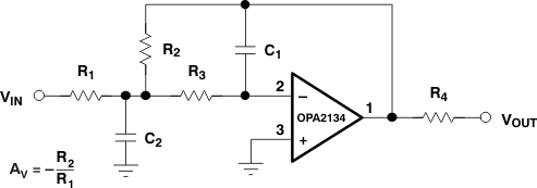 Figure 31. Dual-Supply Filter Circuit
9.2.2 Detailed Design Procedure
This section provides information on how to measure key dynamic performance parameters for the PCM175x-Q1 family of devices. In all cases, an Audio Precision System Two Cascade audio measurement system or equivalent is used to perform the testing.
9.2.2.1 Total Harmonic Distortion + Noise
Total harmonic distortion + noise (THD+N) is a significant figure of merit for audio DAC because it takes into account both harmonic distortion and all noise sources within a specified measurement bandwidth. The average value of the distortion and noise is referred to as THD+N.
For the PCM175x-Q1 family of devices, THD+N is measured with a full-scale, 1-kHz digital sine wave as the test stimulus at the input of the DAC (see Figure 33). The digital generator is set to 24-bit audio word length and a sampling frequency of 44.1 kHz or 96 kHz. The digital generator output is taken from the unbalanced S/PDIF connector of the measurement system. The S/PDIF data is transmitted through a coaxial cable to the digital audio receiver on the DEM-DAI1753 demonstration board. The receiver is then configured to output 24-bit data in either I2S or left-justified data format. The DAC audio interface format is programmed to match the receiver output format. The analog output is then taken from the DAC post filter and connected to the analog analyzer input of the measurement system. The analog input is band limited using filters resident in the analyzer. The resulting THD+N is measured by the analyzer and displayed by the measurement system.
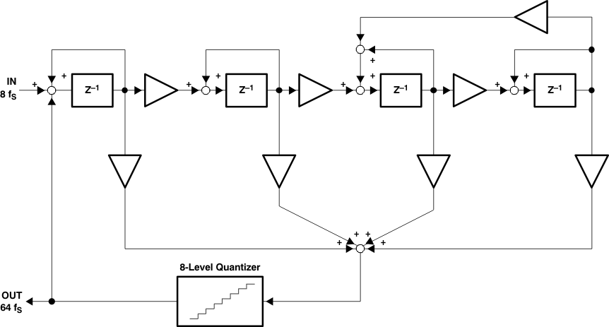 Figure 32. Eight-Level Delta-Sigma Modulator
9.2.2.2 Dynamic Range
Dynamic range is specified as A-weighted THD+N measured with a –60-dB full-scale, 1-kHz digital sine wave stimulus at the input of the DAC. This measurement is designed to give a good indicator of how the DAC performs given a low-level input signal.
The measurement setup for the dynamic range measurement is shown in Figure 34, and is similar to the THD+N test setup discussed previously. The differences include the band limit filter selection, the additional A-weighting filter, and the –60-dB full-scale input level.
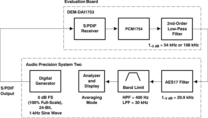 Figure 33. Test Setup for THD+N Measurement
9.2.2.3 Idle Channel Signal-to-Noise Ratio (SNR)
The SNR test provides a measure of the noise floor of the DAC. The input to the DAC is all–0s data, and the dither function of the digital generator must be disabled to ensure an all–0s data stream at the input of the DAC.
The measurement setup for SNR is identical to that used for dynamic range, with the exception of the input signal level.
See the note provided in Figure 34.
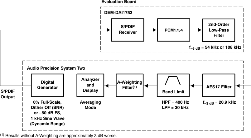 Figure 34. Test Setup for Dynamic Range and SNR Measurement
9.2.3 Application Curves
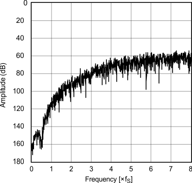
| Quantization noise spectrum (×64 oversampling) |
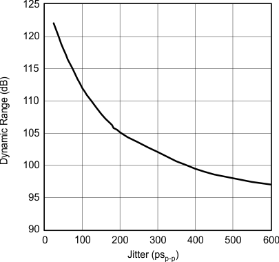
| Jitter dependence (×64 oversampling) |
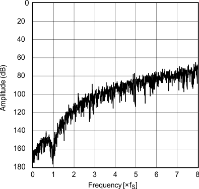
| Quantization noise spectrum (×128 oversampling) |