SLES142B JUNE 2005 – July 2016 PCM1803A
PRODUCTION DATA.
- 1 Features
- 2 Applications
- 3 Description
- 4 Revision History
- 5 Pin Configuration and Functions
- 6 Specifications
- 7 Detailed Description
- 8 Application and Implementation
- 9 Power Supply Recommendations
- 10Layout
- 11Device and Documentation Support
- 12Mechanical, Packaging, and Orderable Information
Package Options
Mechanical Data (Package|Pins)
- DB|20
Thermal pad, mechanical data (Package|Pins)
Orderable Information
6 Specifications
6.1 Absolute Maximum Ratings
over operating free-air temperature range (unless otherwise noted)(1)| MIN | MAX | UNIT | ||
|---|---|---|---|---|
| Supply voltage | VCC | –0.3 | 6.5 | V |
| VDD | –0.3 | 4 | ||
| Ground voltage differences | AGND, DGND | ±0.1 | V | |
| Digital input voltage, VI | LRCK, BCK, DOUT | –0.3 | (VDD + 0.3) < 4 | V |
| PDWN, BYPAS, TEST, SCKI, OSR, FMT0, FMT1, MODE0, MODE1 | –0.3 | 6.5 | ||
| Analog input voltage, VI | VINL, VINR, VREF1, VREF2 | –0.3 | (VCC + 0.3) < 6.5 | V |
| Input current, II | Any pins except supplies | ±10 | mA | |
| Ambient temperature under bias, Tbias | –40 | 125 | °C | |
| Junction temperature, TJ | 150 | °C | ||
| Lead temperature (soldering) | 5 s | 260 | °C | |
| Package temperature (IR reflow, peak) | 260 | °C | ||
| Storage temperature, Tstg | –55 | 150 | °C | |
(1) Stresses beyond those listed under Absolute Maximum Ratings may cause permanent damage to the device. These are stress ratings only, which do not imply functional operation of the device at these or any other conditions beyond those indicated under Recommended Operating Conditions. Exposure to absolute-maximum-rated conditions for extended periods may affect device reliability.
6.2 ESD Ratings
| VALUE | UNIT | |||
|---|---|---|---|---|
| V(ESD) | Electrostatic discharge | Human-body model (HBM), per ANSI/ESDA/JEDEC JS-001(1) | ±4000 | V |
| Charged-device model (CDM), per JEDEC specification JESD22-C101(2) | ±1500 | |||
(1) JEDEC document JEP155 states that 500-V HBM allows safe manufacturing with a standard ESD control process.
(2) JEDEC document JEP157 states that 250-V CDM allows safe manufacturing with a standard ESD control process.
6.3 Recommended Operating Conditions
over operating free-air temperature range| MIN | NOM | MAX | UNIT | ||
|---|---|---|---|---|---|
| Analog supply voltage, VCC | 4.5 | 5 | 5.5 | V | |
| Digital supply voltage, VDD | 2.7 | 3.3 | 3.6 | V | |
| Analog input voltage, full-scale (–0 dB) | 3 | Vp-p | |||
| Digital input logic family | TTL | ||||
| Digital input clock frequency | System clock | 8.192 | 49.152 | MHz | |
| Sampling clock | 32 | 96 | kHz | ||
| Digital output load capacitance | 20 | pF | |||
| Operating free-air temperature, TA | –25 | 85 | °C | ||
6.4 Thermal Information
| THERMAL METRIC(1) | PCM1803A | UNIT | |
|---|---|---|---|
| DB (SSOP) | |||
| 20 PINS | |||
| RθJA | Junction-to-ambient thermal resistance | 84.4 | °C/W |
| RθJC(top) | Junction-to-case (top) thermal resistance | 42.4 | °C/W |
| RθJB | Junction-to-board thermal resistance | 41.4 | °C/W |
| ψJT | Junction-to-top characterization parameter | 8.3 | °C/W |
| ψJB | Junction-to-board characterization parameter | 40.7 | °C/W |
| RθJC(bot) | Junction-to-case (bottom) thermal resistance | — | °C/W |
(1) For more information about traditional and new thermal metrics, see the Semiconductor and IC Package Thermal Metrics application report.
6.5 Electrical Characteristics
All specifications at TA = 25°C, VCC = 5 V, VDD = 3.3 V, master mode, fS = 44.1 kHz, system clock = 384 fS,oversampling ratio = ×128, 24-bit data (unless otherwise noted)
| PARAMETER | TEST CONDITIONS | MIN | TYP | MAX | UNIT | |
|---|---|---|---|---|---|---|
| Resolution | 24 | Bits | ||||
| DATA FORMAT | ||||||
| Audio data interface format | Left-justified, I2S, right-justified | |||||
| Audio data bit length | 20, 24 | Bits | ||||
| Audio data format | MSB-first, 2s complement | |||||
| fS | Sampling frequency | 16 | 44.1 | 96 | kHz | |
| System clock frequency | 256 fS | 4.096 | 11.2896 | 24.576 | MHz | |
| 384 fS | 6.144 | 16.9344 | 36.864 | |||
| 512 fS | 8.192 | 22.5792 | 49.152 | |||
| 768 fS | 12.288 | 33.8688 | ||||
| INPUT LOGIC | ||||||
| VIH (1) | Input logic-level voltage | 2 | VDD | Vdc | ||
| VIL (1) | 0 | 0.8 | ||||
| VIH (2) (3) | 2 | 5.5 | ||||
| VIL (2) (3) | 0 | 0.8 | ||||
| IIH (1) (2) | Input logic-level current | VIN = VDD | ±10 | μA | ||
| IIL (1) (2) | VIN = 0 | ±10 | ||||
| IIH (3) | VIN = VDD | 65 | 100 | |||
| IIL (3) | VIN = 0 | ±10 | ||||
| OUTPUT LOGIC | ||||||
| VOH (4) | Output logic-level voltage | IOUT = –4 mA | 2.8 | Vdc | ||
| VOL (4) | IOUT = 4 mA | 0.5 | ||||
| DC ACCURACY | ||||||
| Gain mismatch, channel-to-channel | ±1 | ±3 | % of FSR | |||
| Gain error | ±2 | ±4 | % of FSR | |||
| Bipolar zero error | HPF bypass | ±0.4 | % of FSR | |||
| DYNAMIC PERFORMANCE(5) | ||||||
| THD+N | Total harmonic distortion + noise | VIN = –0.5 dB, fS = 44.1 kHz | –95 | –89 | dB | |
| VIN = –0.5 dB, fS = 96 kHz(6) | –93 | |||||
| VIN = –60 dB, fS = 44.1 kHz | –41 | |||||
| VIN = –60 dB, fS = 96 kHz(6) | –41 | |||||
| Dynamic range | fS = 44.1 kHz, A-weighted | 100 | 103 | dB | ||
| fS = 96 kHz, A-weighted(6) | 103 | |||||
| SNR | Signal-to-noise ratio | fS = 44.1 kHz, A-weighted | 100 | 103 | dB | |
| fS = 96 kHz, A-weighted(6) | 103 | |||||
| Channel separation | fS = 44.1 kHz | 95 | 98 | dB | ||
| fS = 96 kHz(6) | 99 | |||||
| ANALOG INPUT | ||||||
| VI | Input voltage | 0.6 × VCC | Vp-p | |||
| Center voltage (VREF1) | 0.5 × VCC | V | ||||
| Input impedance | 40 | kΩ | ||||
| DIGITAL FILTER PERFORMANCE | ||||||
| Pass band | 0.454 × fS | Hz | ||||
| Stop band | 0.583 × fS | Hz | ||||
| Pass-band ripple | ±0.05 | dB | ||||
| Stop-band attenuation | –65 | dB | ||||
| tGD | Group delay time | 17.4 / fS | s | |||
| HPF frequency response | –3 dB | 0.019 × fS | mHz | |||
| POWER SUPPLY REQUIREMENTS | ||||||
| VCC | Supply voltage range | 4.5 | 5 | 5.5 | Vdc | |
| VDD | 2.7 | 3.3 | 3.6 | Vdc | ||
| ICC | Supply current(7) | 7.7 | 10 | mA | ||
| Power down(8) | 5 | μA | ||||
| IDD | fS = 44.1 kHz | 6.5 | 9 | mA | ||
| fS = 96 kHz (6) | 11.7 | mA | ||||
| Power down(8) | 1 | μA | ||||
| Power dissipation | fS = 44.1 kHz | 60 | 80 | mW | ||
| fS = 96 kHz (6) | 77 | mW | ||||
| Power down(8) | 28 | μW | ||||
| TEMPERATURE RANGE | ||||||
| TA | Operating free-air temperature | –40 | 85 | °C | ||
(1) Pins 10 to 11: LRCK, BCK (Schmitt-trigger input, in slave mode)
(2) Pin 15: SCKI (Schmitt-trigger input, 5-V tolerant)
(3) Pins 7 to 9, 16 to 20: PDWN, BYPAS, TEST, OSR, FMT0, FMT1, MODE0, MODE1 (Schmitt-trigger input, with 50-kΩ typical pulldown resistor, 5-V tolerant)
(4) Pins 10 to 12: LRCK, BCK (in master mode), DOUT
(5) Analog performance specifications are tested using the System Two™ audio measurement system by Audio Precision™, using 400-Hz HPF, 20-kHz LPF in rms mode.
(6) fS = 96 kHz, system clock = 256 fS, oversampling ratio = ×64.
(7) Minimum load on DOUT (pin 12), BCK (pin 11), LRCK (pin 10)
(8) Halt SCKI, BCK, LRCK
6.6 Typical Characteristics
6.6.1 Typical Curves of Internal Filter
6.6.1.1 Decimation Filter Frequency Response
All specifications at TA = 25°C, VCC = 5 V, VDD = 3.3 V, master mode, fS = 44.1 kHz, system clock = 384 fS,
oversampling ratio = ×128, 24-bit data (unless otherwise noted)
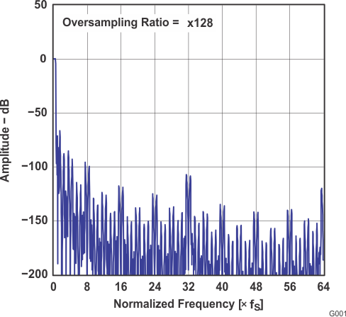 Figure 1. Overall Characteristics
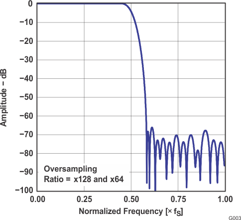 Figure 3. Stop-Band Attenuation Characteristics
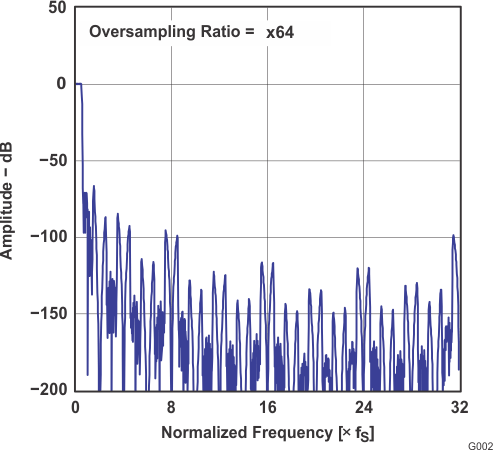 Figure 2. Overall Characteristics
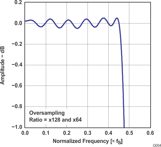 Figure 4. Pass-Band Ripple Characteristics
6.6.1.2 Low-Cut Filter Frequency Response
All specifications at TA = 25°C, VCC = 5 V, VDD = 3.3 V, master mode, fS = 44.1 kHz, system clock = 384 fS,oversampling ratio = ×128, 24-bit data (unless otherwise noted)
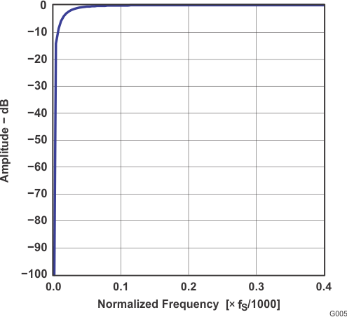 Figure 5. HPF Stop-Band Characteristics
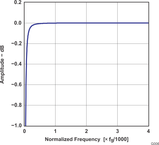 Figure 6. HPF Pass-Band Characteristics
6.6.2 Typical Performance Curves
All specifications at TA = 25°C, VCC = 5 V, VDD = 3.3 V, master mode, fS = 44.1 kHz, system clock = 384 fS,oversampling ratio = ×128, 24-bit data (unless otherwise noted)
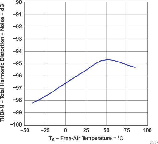 Figure 7. Total Harmonic Distortion + Noise vs Temperature
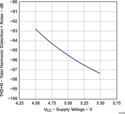 Figure 9. Total Harmonic Distortion + Noise vs Supply Voltage
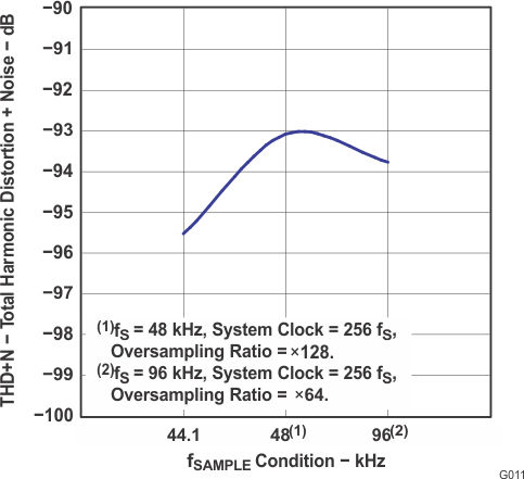 Figure 11. Total Harmonic Distortion + Noise vs fSAMPLE Condition
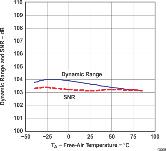 Figure 8. Dynamic Range and Signal-to-Noise Ratio vs Temperature
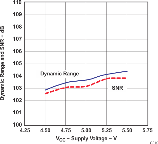 Figure 10. Dynamic Range and Signal-to-Noise Ratio vs Supply Voltage
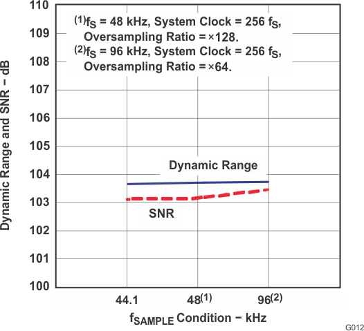 Figure 12. Dynamic Range and Signal-to-Noise Ratio vs fSAMPLE Condition
6.6.3 Output Spectrum
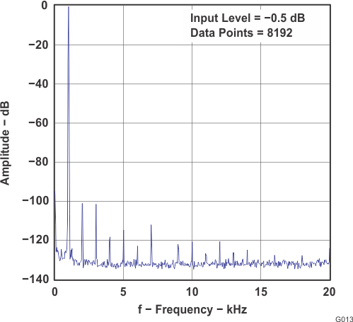 Figure 13. Output Spectrum
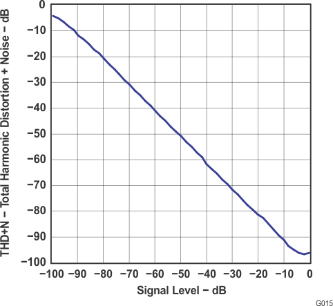 Figure 15. Total Harmonic Distortion + Noise vs Signal Level
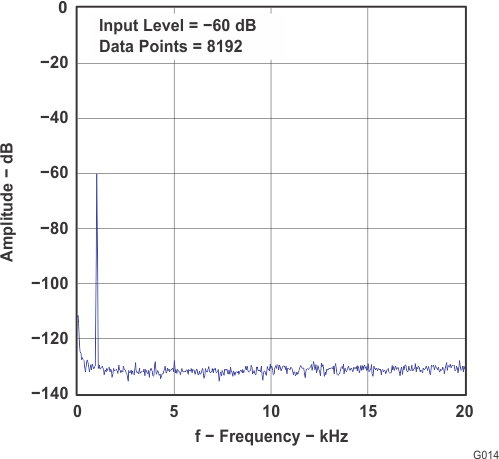 Figure 14. Output Spectrum
6.6.4 Supply Current
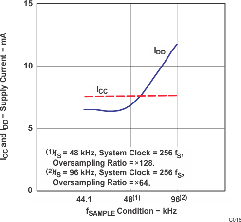 Figure 16. Supply Current vs fSAMPLE Condition