SBASA61A December 2020 – June 2021 PCM1820 , PCM1821
PRODUCTION DATA
- 1 Features
- 2 Applications
- 3 Description
- 4 Revision History
- 5 Device Comparison Table
- 6 Pin Configuration and Functions
- 7 Specifications
-
8 Detailed Description
- 8.1 Overview
- 8.2 Functional Block Diagram
- 8.3
Feature Description
- 8.3.1 Hardware Control
- 8.3.2 Audio Serial Interfaces
- 8.3.3 Phase-Locked Loop (PLL) and Clock Generation
- 8.3.4 Input Channel Configurations
- 8.3.5 Reference Voltage
- 8.3.6
Signal-Chain Processing
- 8.3.6.1 Digital High-Pass Filter
- 8.3.6.2
Configurable Digital Decimation Filters
- 8.3.6.2.1
Linear Phase Filters
- 8.3.6.2.1.1 Sampling Rate: 8 kHz or 7.35 kHz
- 8.3.6.2.1.2 Sampling Rate: 16 kHz or 14.7 kHz
- 8.3.6.2.1.3 Sampling Rate: 24 kHz or 22.05 kHz
- 8.3.6.2.1.4 Sampling Rate: 32 kHz or 29.4 kHz
- 8.3.6.2.1.5 Sampling Rate: 48 kHz or 44.1 kHz
- 8.3.6.2.1.6 Sampling Rate: 96 kHz or 88.2 kHz
- 8.3.6.2.1.7 Sampling Rate: 192 kHz or 176.4 kHz
- 8.3.6.2.2 Low-Latency Filters
- 8.3.6.2.1
Linear Phase Filters
- 8.3.7 Dynamic Range Enhancer (DRE)
- 8.4 Device Functional Modes
- 9 Application and Implementation
- 10Power Supply Recommendations
- 11Layout
- 12Device and Documentation Support
- 13Mechanical, Packaging, and Orderable Information
Package Options
Mechanical Data (Package|Pins)
- RTE|20
Thermal pad, mechanical data (Package|Pins)
Orderable Information
8.3.6.1 Digital High-Pass Filter
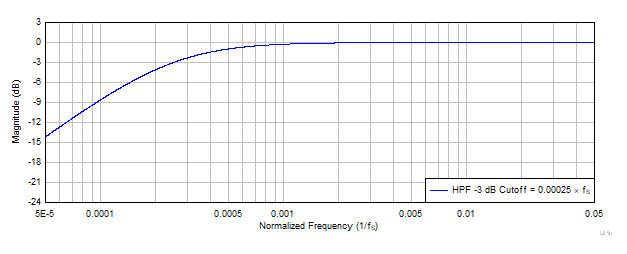
To remove the DC offset component and attenuate the undesired low-frequency noise content in the record data, the device supports a fixed high-pass filter (HPF) with –3-dB cut-off frequency of 0.00025 × fS. The HPF is not a channel-independent filter but is globally applicable for all the ADC channels. This HPF is constructed using the first-order infinite impulse response (IIR) filter, and is efficient enough to filter out possible DC components of the signal. Table 8-6 shows the fixed –3-dB cutoff frequency value. Figure 8-6 shows a frequency response plot for the HPF filter.
| –3-dB CUTOFF FREQUENCY VALUE | -3-dB CUTTOFF FREQUENCY AT 16 kHz SAMPLE RATE | -3-dB CUTTOFF FREQUENCY AT 48 kHz SAMPLE RATE |
|---|---|---|
| 0.00025 × fS | 4 Hz | 12 Hz |
 Figure 8-6 HPF
Filter Frequency Response Plot