SBASAH0A April 2022 – September 2022 PCM3120-Q1
PRODUCTION DATA
- 1 Features
- 2 Applications
- 3 Description
- 4 Revision History
- 5 Device Comparison Table
- 6 Pin Configuration and Functions
-
7 Specifications
- 7.1 Absolute Maximum Ratings
- 7.2 ESD Ratings
- 7.3 Recommended Operating Conditions
- Thermal Information
- 7.4 Electrical Characteristics
- 7.5 Timing Requirements: I2C Interface
- 7.6 Switching Characteristics: I2C Interface
- 7.7 Timing Requirements: TDM, I2S or LJ Interface
- 7.8 Switching Characteristics: TDM, I2S or LJ Interface
- Timing Requirements: PDM Digital Microphone Interface
- 7.9 Switching Characteristics: PDM Digial Microphone Interface
- 7.10 Timing Diagrams
- 7.11 Typical Characteristics
-
8 Detailed Description
- 8.1 Overview
- 8.2 Functional Block Diagram
- 8.3
Feature Description
- 8.3.1 Serial Interfaces
- 8.3.2 Phase-Locked Loop (PLL) and Clock Generation
- 8.3.3 Input Channel Configurations
- 8.3.4 Reference Voltage
- 8.3.5 Programmable Microphone Bias
- 8.3.6
Signal-Chain Processing
- 8.3.6.1 Programmable Channel Gain and Digital Volume Control
- 8.3.6.2 Programmable Channel Gain Calibration
- 8.3.6.3 Programmable Channel Phase Calibration
- 8.3.6.4 Programmable Digital High-Pass Filter
- 8.3.6.5 Programmable Digital Biquad Filters
- 8.3.6.6 Programmable Channel Summer and Digital Mixer
- 8.3.6.7
Configurable Digital Decimation Filters
- 8.3.6.7.1
Linear Phase Filters
- 8.3.6.7.1.1 Sampling Rate: 7.35 kHz to 8 kHz
- 8.3.6.7.1.2 Sampling Rate: 14.7 kHz to 16 kHz
- 8.3.6.7.1.3 Sampling Rate: 22.05 kHz to 24 kHz
- 8.3.6.7.1.4 Sampling Rate: 29.4 kHz to 32 kHz
- 8.3.6.7.1.5 Sampling Rate: 44.1 kHz to 48 kHz
- 8.3.6.7.1.6 Sampling Rate: 88.2 kHz to 96 kHz
- 8.3.6.7.1.7 Sampling Rate: 176.4 kHz to 192 kHz
- 8.3.6.7.1.8 Sampling Rate: 352.8 kHz to 384 kHz
- 8.3.6.7.1.9 Sampling Rate: 705.6 kHz to 768 kHz
- 8.3.6.7.2 Low-Latency Filters
- 8.3.6.7.3
Ultra-Low Latency Filters
- 8.3.6.7.3.1 Sampling Rate: 14.7 kHz to 16 kHz
- 8.3.6.7.3.2 Sampling Rate: 22.05 kHz to 24 kHz
- 8.3.6.7.3.3 Sampling Rate: 29.4 kHz to 32 kHz
- 8.3.6.7.3.4 Sampling Rate: 44.1 kHz to 48 kHz
- 8.3.6.7.3.5 Sampling Rate: 88.2 kHz to 96 kHz
- 8.3.6.7.3.6 Sampling Rate: 176.4 kHz to 192 kHz
- 8.3.6.7.3.7 Sampling Rate: 352.8 kHz to 384 kHz
- 8.3.6.7.1
Linear Phase Filters
- 8.3.7 Automatic Gain Controller (AGC)
- 8.3.8 Voice Activity Detection (VAD)
- 8.3.9 Digital PDM Microphone Record Channel
- 8.3.10 Interrupts, Status, and Digital I/O Pin Multiplexing
- 8.4 Device Functional Modes
- 8.5 Programming
- 8.6 Register Maps
- 9 Application and Implementation
- 10Power Supply Recommendations
- 11Layout
- 12Device and Documentation Support
- 13Mechanical, Packaging, and Orderable Information
Package Options
Mechanical Data (Package|Pins)
- RTE|20
Thermal pad, mechanical data (Package|Pins)
Orderable Information
8.3.6.7.2.4 Sampling Rate: 44.1 kHz to 48 kHz
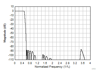
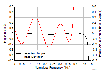
Figure 8-43 shows the magnitude response and Figure 8-44 shows the pass-band ripple and phase deviation for a decimation filter with a sampling rate of 44.1 kHz to 48 kHz. Table 8-35 lists the specifications for a decimation filter with a 44.1-kHz to 48-kHz sampling rate.
 Figure 8-43 Low-Latency Decimation Filter Magnitude Response
 Figure 8-44 Low-Latency Decimation Filter Pass-Band Ripple and Phase Deviation
Table 8-35 Low-Latency Decimation Filter Specifications
| PARAMETER | TEST CONDITIONS | MIN | TYP | MAX | UNIT |
|---|---|---|---|---|---|
| Pass-band ripple | Frequency range is 0 to 0.452 × fS | –0.015 | 0.015 | dB | |
| Stop-band attenuation | Frequency range is 0.6 × fS onwards | 86.4 | dB | ||
| Group delay or latency | Frequency range is 0 to 0.365 × fS | 7.7 | 1/fS | ||
| Group delay deviation | Frequency range is 0 to 0.365 × fS | –0.027 | 0.027 | 1/fS | |
| Phase deviation | Frequency range is 0 to 0.365 × fS | –0.25 | 0.30 | Degrees |