SLAS859C May 2012 – May 2015 PCM5100A , PCM5100A-Q1 , PCM5101A , PCM5101A-Q1 , PCM5102A , PCM5102A-Q1
PRODUCTION DATA.
- 1 Features
- 2 Applications
- 3 Description
- 4 Simplified System Diagram
- 5 Revision History
- 6 Device Comparison
- 7 Pin Configuration and Functions
- 8 Specifications
- 9 Detailed Description
- 10Applications and Implementation
- 11Power Supply Recommendations
- 12Layout
- 13Device and Documentation Support
- 14Mechanical, Packaging, and Orderable Information
Package Options
Mechanical Data (Package|Pins)
- PW|20
Thermal pad, mechanical data (Package|Pins)
Orderable Information
10 Applications and Implementation
NOTE
Information in the following applications sections is not part of the TI component specification, and TI does not warrant its accuracy or completeness. TI’s customers are responsible for determining suitability of components for their purposes. Customers should validate and test their design implementation to confirm system functionality.
10.1 Application Information
10.1.1 Typical Applications
10.1.1.1 Example Design Requirements
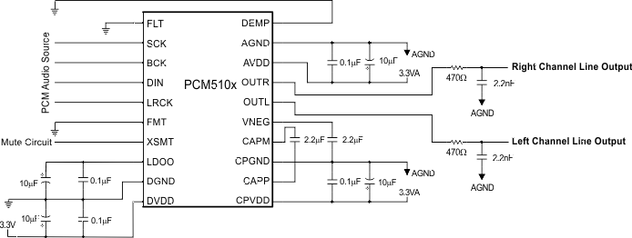
- Device control method: hardware control
- Normal filter latency
- I2S digital audio interface
- Power rail monitoring from the system 12-V rail to mute early on system power loss
- Single-ended 2.1-VRMS analog outputs
- 3-wire I2S interface (BCK PLL)
- Single 3.3-V supply
10.1.1.2 Detailed Design Procedure
- Device control method: See Pin Configuration and Functions and Audio Processing.
- Normal filter latency: FLT pin tied low
- Audio format selection: FMT pin tied low
- Clock and PLL setup (See Reset and System Clock Functions). Ensure incoming BCK meets minimum requirements.
- XSMT pin setup for 12-V monitoring (See External Power Sense Undervoltage Protection Mode).
- Single-supply 3.3-V operation (See Setting Digital Power Supplies and I/O Voltage Rails)
10.1.1.3 Application Curve
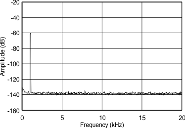
 Figure 34. PCM5101A FFT Plot, DC to 20 kHz with a 1 kHz, –60dBFS Input
