SBASA12 December 2020 PCM6020-Q1
PRODUCTION DATA
- 1 Features
- 2 Applications
- 3 Description
- 4 Revision History
- 5 Device Comparison Table
- 6 Pin Configuration and Functions
-
7 Specifications
- 7.1 Absolute Maximum Ratings
- 7.2 ESD Ratings
- 7.3 Recommended Operating Conditions
- 7.4 Thermal Information
- 7.5 Electrical Characteristics
- 7.6 Timing Requirements: I2C Interface
- 7.7 Switching Characteristics: I2C Interface
- 7.8 Timing Requirements: SPI Interface
- 7.9 Switching Characteristics: SPI Interface
- 7.10 Timing Requirements: TDM, I2S or LJ Interface
- 7.11 Switching Characteristics: TDM, I2S or LJ Interface
- 7.12 Timing Diagrams
- 7.13 Typical Characteristics
-
8 Detailed Description
- 8.1 Overview
- 8.2 Functional Block Diagram
- 8.3
Feature Description
- 8.3.1 Serial Interfaces
- 8.3.2 Phase-Locked Loop (PLL) and Clock Generation
- 8.3.3 Input Channel Configuration
- 8.3.4 Reference Voltage
- 8.3.5 Microphone Bias
- 8.3.6 Input DC Fault Diagnostics
- 8.3.7
Signal-Chain Processing
- 8.3.7.1 Programmable Channel Gain and Digital Volume Control
- 8.3.7.2 Programmable Channel Gain Calibration
- 8.3.7.3 Programmable Channel Phase Calibration
- 8.3.7.4 Programmable Digital High-Pass Filter
- 8.3.7.5 Programmable Digital Biquad Filters
- 8.3.7.6 Programmable Channel Summer and Digital Mixer
- 8.3.7.7
Configurable Digital Decimation Filters
- 8.3.7.7.1
Linear Phase Filters
- 8.3.7.7.1.1 Sampling Rate: 8 kHz or 7.35 kHz
- 8.3.7.7.1.2 Sampling Rate: 16 kHz or 14.7 kHz
- 8.3.7.7.1.3 Sampling Rate: 24 kHz or 22.05 kHz
- 8.3.7.7.1.4 Sampling Rate: 32 kHz or 29.4 kHz
- 8.3.7.7.1.5 Sampling Rate: 48 kHz or 44.1 kHz
- 8.3.7.7.1.6 Sampling Rate: 96 kHz or 88.2 kHz
- 8.3.7.7.1.7 Sampling Rate: 192 kHz or 176.4 kHz
- 8.3.7.7.1.8 Sampling Rate: 384 kHz or 352.8 kHz
- 8.3.7.7.1.9 Sampling Rate: 768 kHz or 705.6 kHz
- 8.3.7.7.2 Low-Latency Filters
- 8.3.7.7.3
Ultra-Low-Latency Filters
- 8.3.7.7.3.1 Sampling Rate: 16 kHz or 14.7 kHz
- 8.3.7.7.3.2 Sampling Rate: 24 kHz or 22.05 kHz
- 8.3.7.7.3.3 Sampling Rate: 32 kHz or 29.4 kHz
- 8.3.7.7.3.4 Sampling Rate: 48 kHz or 44.1 kHz
- 8.3.7.7.3.5 Sampling Rate: 96 kHz or 88.2 kHz
- 8.3.7.7.3.6 Sampling Rate: 192 kHz or 176.4 kHz
- 8.3.7.7.3.7 Sampling Rate: 384 kHz or 352.8 kHz
- 8.3.7.7.1
Linear Phase Filters
- 8.3.8 Automatic Gain Controller (AGC)
- 8.3.9 Interrupts, Status, and Digital I/O Pin Multiplexing
- 8.4 Device Functional Modes
- 8.5 Programming
- 8.6 Register Maps
- 9 Application and Implementation
- 10Power Supply Recommendations
- 11Layout
- 12Device and Documentation Support
Package Options
Mechanical Data (Package|Pins)
- RTV|32
Thermal pad, mechanical data (Package|Pins)
Orderable Information
3 Description
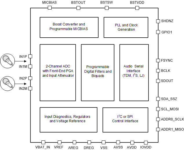
The PCM6020-Q1 is a 2-channel high-performance, audio analog-to-digital converter (ADC) that supports analog input signals up to 10 VRMS. The PCM6020-Q1 supports line and microphone inputs, and allows for both single-ended and differential input configurations. This device offers an integrated high-voltage, programmable microphone bias, and input diagnostic circuitry that allows direct connection to microphone-based automotive systems with full fault diagnostic capability for direct-coupled inputs. The PCM6020-Q1 integrates an efficient boost converter to generate a high voltage microphone bias using an external, low-voltage, 3.3-V supply, which is a readily available supply in the system to generate the high-voltage, programmable microphone bias. The PCM6020-Q1 integrates the programable channel gain, digital volume control, a low-jitter phase-locked loop (PLL), a programmable high-pass filter (HPF), biquad filters, low-latency filter modes, and allows for sample rates up to 768 kHz. The PCM6020-Q1 supports time-division multiplexing (TDM), I2S, or left-justified (LJ) audio formats, and can be controlled with either the I2C or SPI interface. These integrated high-performance features, along with a single, 3.3-V supply operation, make the PCM6020-Q1 device along with PCM6xx0-Q1 device family an excellent choice for scalable, space-constrained automotive systems. The PCM6020-Q1 is part of a larger PCM6xx0-Q1 device family, available for download at ti.com.
| PART NUMBER | PACKAGE | BODY SIZE (NOM) |
|---|---|---|
| PCM6020-Q1 | WQFN (32) | 5.00 mm x 5.00 mm with 0.5-mm pitch |
 Simplified Application Diagram