SBASA12 December 2020 PCM6020-Q1
PRODUCTION DATA
- 1 Features
- 2 Applications
- 3 Description
- 4 Revision History
- 5 Device Comparison Table
- 6 Pin Configuration and Functions
-
7 Specifications
- 7.1 Absolute Maximum Ratings
- 7.2 ESD Ratings
- 7.3 Recommended Operating Conditions
- 7.4 Thermal Information
- 7.5 Electrical Characteristics
- 7.6 Timing Requirements: I2C Interface
- 7.7 Switching Characteristics: I2C Interface
- 7.8 Timing Requirements: SPI Interface
- 7.9 Switching Characteristics: SPI Interface
- 7.10 Timing Requirements: TDM, I2S or LJ Interface
- 7.11 Switching Characteristics: TDM, I2S or LJ Interface
- 7.12 Timing Diagrams
- 7.13 Typical Characteristics
-
8 Detailed Description
- 8.1 Overview
- 8.2 Functional Block Diagram
- 8.3
Feature Description
- 8.3.1 Serial Interfaces
- 8.3.2 Phase-Locked Loop (PLL) and Clock Generation
- 8.3.3 Input Channel Configuration
- 8.3.4 Reference Voltage
- 8.3.5 Microphone Bias
- 8.3.6 Input DC Fault Diagnostics
- 8.3.7
Signal-Chain Processing
- 8.3.7.1 Programmable Channel Gain and Digital Volume Control
- 8.3.7.2 Programmable Channel Gain Calibration
- 8.3.7.3 Programmable Channel Phase Calibration
- 8.3.7.4 Programmable Digital High-Pass Filter
- 8.3.7.5 Programmable Digital Biquad Filters
- 8.3.7.6 Programmable Channel Summer and Digital Mixer
- 8.3.7.7
Configurable Digital Decimation Filters
- 8.3.7.7.1
Linear Phase Filters
- 8.3.7.7.1.1 Sampling Rate: 8 kHz or 7.35 kHz
- 8.3.7.7.1.2 Sampling Rate: 16 kHz or 14.7 kHz
- 8.3.7.7.1.3 Sampling Rate: 24 kHz or 22.05 kHz
- 8.3.7.7.1.4 Sampling Rate: 32 kHz or 29.4 kHz
- 8.3.7.7.1.5 Sampling Rate: 48 kHz or 44.1 kHz
- 8.3.7.7.1.6 Sampling Rate: 96 kHz or 88.2 kHz
- 8.3.7.7.1.7 Sampling Rate: 192 kHz or 176.4 kHz
- 8.3.7.7.1.8 Sampling Rate: 384 kHz or 352.8 kHz
- 8.3.7.7.1.9 Sampling Rate: 768 kHz or 705.6 kHz
- 8.3.7.7.2 Low-Latency Filters
- 8.3.7.7.3
Ultra-Low-Latency Filters
- 8.3.7.7.3.1 Sampling Rate: 16 kHz or 14.7 kHz
- 8.3.7.7.3.2 Sampling Rate: 24 kHz or 22.05 kHz
- 8.3.7.7.3.3 Sampling Rate: 32 kHz or 29.4 kHz
- 8.3.7.7.3.4 Sampling Rate: 48 kHz or 44.1 kHz
- 8.3.7.7.3.5 Sampling Rate: 96 kHz or 88.2 kHz
- 8.3.7.7.3.6 Sampling Rate: 192 kHz or 176.4 kHz
- 8.3.7.7.3.7 Sampling Rate: 384 kHz or 352.8 kHz
- 8.3.7.7.1
Linear Phase Filters
- 8.3.8 Automatic Gain Controller (AGC)
- 8.3.9 Interrupts, Status, and Digital I/O Pin Multiplexing
- 8.4 Device Functional Modes
- 8.5 Programming
- 8.6 Register Maps
- 9 Application and Implementation
- 10Power Supply Recommendations
- 11Layout
- 12Device and Documentation Support
Package Options
Mechanical Data (Package|Pins)
- RTV|32
Thermal pad, mechanical data (Package|Pins)
Orderable Information
8.3.8 Automatic Gain Controller (AGC)
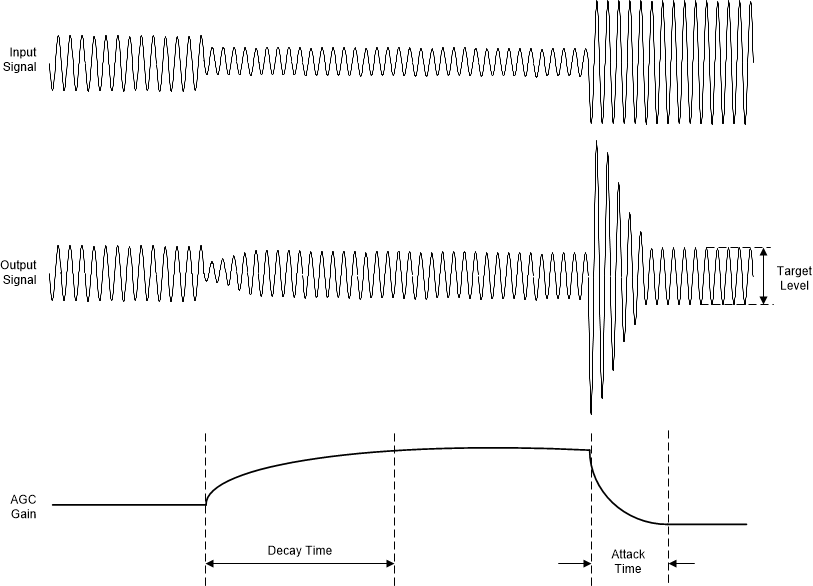
The device includes an automatic gain controller (AGC) for ADC recording that must be used only for the AC-coupled input configuration. As shown in Figure 8-65, the AGC can be used to maintain a nominally constant output level when recording speech. Instead of manually setting the channel gain in AGC mode, the circuitry automatically adjusts the channel gain when the input signal becomes overly loud or very weak, such as when a person speaking into a microphone moves closer to or farther from the microphone. The AGC algorithm has several programmable parameters, including target level, maximum gain allowed, attack and release (or decay) time constants, and noise thresholds that allow the algorithm to be fine-tuned for any particular application.
 Figure 8-65 AGC Characteristics
The target level (AGC_LVL) represents the nominal output level at which the AGC attempts to hold the ADC output signal level. The PCM6020-Q1 allows programming of different target levels, which can be programmed from –6 dB to –36 dB relative to a full-scale signal, and the AGC_LVL default value is set to –34 dB. The target level is recommended to be set with enough margin to prevent clipping when loud sounds occur. Table 8-42 lists the AGC target level configuration settings.
| P0_R112_D[7:4] : AGC_LVL[3:0] | AGC TARGET LEVEL FOR OUTPUT |
|---|---|
| 0000 | The AGC target level is the –6-dB output signal level |
| 0001 | The AGC target level is the –8-dB output signal level |
| 0010 | The AGC target level is the –10-dB output signal level |
| … | … |
| 1110 (default) | The AGC target level is the –34-dB output signal level |
| 1111 | The AGC target level is the –36-dB output signal level |
The maximum gain allowed (AGC_MAXGAIN) gives flexibility to the designer to restrict the maximum gain applied by the AGC. This feature limits the channel gain in situations where environmental noise is greater than the programmed noise threshold. The AGC_MAXGAIN can be programmed from 3 dB to 42 dB with steps of 3 dB and the default value is set to 24 dB. Table 8-43 lists the AGC_MAXGAIN configuration settings.
| P0_R112_D[3:0] : AGC_MAXGAIN[3:0] | AGC MAXIMUM GAIN ALLOWED |
|---|---|
| 0000 | The AGC maximum gain allowed is 3 dB |
| 0001 | The AGC maximum gain allowed is 6 dB |
| 0010 | The AGC maximum gain allowed is 9 dB |
| … | … |
| 0111 (default) | The AGC maximum gain allowed is 24 dB |
| … | … |
| 1110 | The AGC maximum gain allowed is 39 dB |
| 1111 | The AGC maximum gain allowed is 42 dB |
For further details on the AGC various configurable parameter and application use, see the Using the Automatic Gain Controller in PCM6xx0-Q1 application report.