SBASA12 December 2020 PCM6020-Q1
PRODUCTION DATA
- 1 Features
- 2 Applications
- 3 Description
- 4 Revision History
- 5 Device Comparison Table
- 6 Pin Configuration and Functions
-
7 Specifications
- 7.1 Absolute Maximum Ratings
- 7.2 ESD Ratings
- 7.3 Recommended Operating Conditions
- 7.4 Thermal Information
- 7.5 Electrical Characteristics
- 7.6 Timing Requirements: I2C Interface
- 7.7 Switching Characteristics: I2C Interface
- 7.8 Timing Requirements: SPI Interface
- 7.9 Switching Characteristics: SPI Interface
- 7.10 Timing Requirements: TDM, I2S or LJ Interface
- 7.11 Switching Characteristics: TDM, I2S or LJ Interface
- 7.12 Timing Diagrams
- 7.13 Typical Characteristics
-
8 Detailed Description
- 8.1 Overview
- 8.2 Functional Block Diagram
- 8.3
Feature Description
- 8.3.1 Serial Interfaces
- 8.3.2 Phase-Locked Loop (PLL) and Clock Generation
- 8.3.3 Input Channel Configuration
- 8.3.4 Reference Voltage
- 8.3.5 Microphone Bias
- 8.3.6 Input DC Fault Diagnostics
- 8.3.7
Signal-Chain Processing
- 8.3.7.1 Programmable Channel Gain and Digital Volume Control
- 8.3.7.2 Programmable Channel Gain Calibration
- 8.3.7.3 Programmable Channel Phase Calibration
- 8.3.7.4 Programmable Digital High-Pass Filter
- 8.3.7.5 Programmable Digital Biquad Filters
- 8.3.7.6 Programmable Channel Summer and Digital Mixer
- 8.3.7.7
Configurable Digital Decimation Filters
- 8.3.7.7.1
Linear Phase Filters
- 8.3.7.7.1.1 Sampling Rate: 8 kHz or 7.35 kHz
- 8.3.7.7.1.2 Sampling Rate: 16 kHz or 14.7 kHz
- 8.3.7.7.1.3 Sampling Rate: 24 kHz or 22.05 kHz
- 8.3.7.7.1.4 Sampling Rate: 32 kHz or 29.4 kHz
- 8.3.7.7.1.5 Sampling Rate: 48 kHz or 44.1 kHz
- 8.3.7.7.1.6 Sampling Rate: 96 kHz or 88.2 kHz
- 8.3.7.7.1.7 Sampling Rate: 192 kHz or 176.4 kHz
- 8.3.7.7.1.8 Sampling Rate: 384 kHz or 352.8 kHz
- 8.3.7.7.1.9 Sampling Rate: 768 kHz or 705.6 kHz
- 8.3.7.7.2 Low-Latency Filters
- 8.3.7.7.3
Ultra-Low-Latency Filters
- 8.3.7.7.3.1 Sampling Rate: 16 kHz or 14.7 kHz
- 8.3.7.7.3.2 Sampling Rate: 24 kHz or 22.05 kHz
- 8.3.7.7.3.3 Sampling Rate: 32 kHz or 29.4 kHz
- 8.3.7.7.3.4 Sampling Rate: 48 kHz or 44.1 kHz
- 8.3.7.7.3.5 Sampling Rate: 96 kHz or 88.2 kHz
- 8.3.7.7.3.6 Sampling Rate: 192 kHz or 176.4 kHz
- 8.3.7.7.3.7 Sampling Rate: 384 kHz or 352.8 kHz
- 8.3.7.7.1
Linear Phase Filters
- 8.3.8 Automatic Gain Controller (AGC)
- 8.3.9 Interrupts, Status, and Digital I/O Pin Multiplexing
- 8.4 Device Functional Modes
- 8.5 Programming
- 8.6 Register Maps
- 9 Application and Implementation
- 10Power Supply Recommendations
- 11Layout
- 12Device and Documentation Support
Package Options
Mechanical Data (Package|Pins)
- RTV|32
Thermal pad, mechanical data (Package|Pins)
Orderable Information
8.3.1.3 Using Multiple Devices With Shared Buses
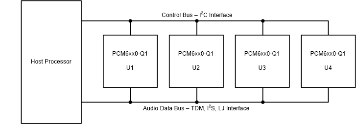
The device has many supported features and flexible options that can be used in the system to seamlessly connect multiple PCM6xx0-Q1 devices by sharing a single common I2C control bus and an audio serial interface bus. This architecture enables multiple applications to be applied to a system that require a microphone array for beam-forming operation, hands-free in-vehicle communication, car cabin active noise cancellation, and so forth. Figure 8-13 shows a diagram of multiple PCM6020-Q1 devices in a configuration where the control and audio data buses are shared.
 Figure 8-13 Multiple PCM6020-Q1 Devices With Shared Control and Audio Data Buses
The PCM6020-Q1 consists of the following features to enable seamless connection and interaction of multiple devices using a shared bus:
- Supports up to four pin-programmable I2C slave addresses
- I2C broadcast simultaneously writes to (or triggers) all PCM6020-Q1 devices
- Supports up to 64 configuration output channel slots for the audio serial interface
- Tri-state feature (with enable and disable) for the unused audio data slots of the device
- Supports a bus-holder feature (with enable and disable) to keep the last driven value on the audio bus
- The GPIOx pin can be configured as a secondary output data lane for the audio serial interface
- The GPIOx or GPIx pin can be used in a daisy-chain configuration of multiple PCM6xx0-Q1 devices
- Supports one BCLK cycle data latching timing to relax the timing requirement for the high-speed interface
- Programmable master and slave options for the audio serial interface
- Ability to synchronize the multiple devices for the simultaneous sampling requirement across devices