SBASA30 December 2020 PCM6480-Q1
PRODUCTION DATA
- 1 Features
- 2 Applications
- 3 Description
- 4 Revision History
- 5 Device Comparison Table
- 6 Pin Configuration and Functions
-
7 Specifications
- 7.1 Absolute Maximum Ratings
- 7.2 ESD Ratings
- 7.3 Recommended Operating Conditions
- 7.4 Thermal Information
- 7.5 Electrical Characteristics
- 7.6 Timing Requirements: I2C Interface
- 7.7 Switching Characteristics: I2C Interface
- 7.8 Timing Requirements: SPI Interface
- 7.9 Switching Characteristics: SPI Interface
- 7.10 Timing Requirements: TDM, I2S or LJ Interface
- 7.11 Switching Characteristics: TDM, I2S or LJ Interface
- 7.12 Timing Requirements: PDM Digital Microphone Interface
- 7.13 Switching Characteristics: PDM Digial Microphone Interface
- 7.14 Timing Diagrams
- 7.15 Typical Characteristics
-
8 Detailed Description
- 8.1 Overview
- 8.2 Functional Block Diagram
- 8.3
Feature Description
- 8.3.1 Serial Interfaces
- 8.3.2 Phase-Locked Loop (PLL) and Clock Generation
- 8.3.3 Analog Input Channel Configuration
- 8.3.4 Reference Voltage
- 8.3.5 Microphone Bias
- 8.3.6 Input DC Fault Diagnostics
- 8.3.7 Digital PDM Microphone Record Channel
- 8.3.8
Signal-Chain Processing
- 8.3.8.1 Programmable Channel Gain and Digital Volume Control
- 8.3.8.2 Programmable Channel Gain Calibration
- 8.3.8.3 Programmable Channel Phase Calibration
- 8.3.8.4 Programmable Digital High-Pass Filter
- 8.3.8.5 Programmable Digital Biquad Filters
- 8.3.8.6 Programmable Channel Summer and Digital Mixer
- 8.3.8.7
Configurable Digital Decimation Filters
- 8.3.8.7.1
Linear Phase Filters
- 8.3.8.7.1.1 Sampling Rate: 8 kHz or 7.35 kHz
- 8.3.8.7.1.2 Sampling Rate: 16 kHz or 14.7 kHz
- 8.3.8.7.1.3 Sampling Rate: 24 kHz or 22.05 kHz
- 8.3.8.7.1.4 Sampling Rate: 32 kHz or 29.4 kHz
- 8.3.8.7.1.5 Sampling Rate: 48 kHz or 44.1 kHz
- 8.3.8.7.1.6 Sampling Rate: 96 kHz or 88.2 kHz
- 8.3.8.7.1.7 Sampling Rate: 192 kHz or 176.4 kHz
- 8.3.8.7.1.8 Sampling Rate: 384 kHz or 352.8 kHz
- 8.3.8.7.1.9 Sampling Rate: 768 kHz or 705.6 kHz
- 8.3.8.7.2 Low-Latency Filters
- 8.3.8.7.3
Ultra-Low-Latency Filters
- 8.3.8.7.3.1 Sampling Rate: 16 kHz or 14.7 kHz
- 8.3.8.7.3.2 Sampling Rate: 24 kHz or 22.05 kHz
- 8.3.8.7.3.3 Sampling Rate: 32 kHz or 29.4 kHz
- 8.3.8.7.3.4 Sampling Rate: 48 kHz or 44.1 kHz
- 8.3.8.7.3.5 Sampling Rate: 96 kHz or 88.2 kHz
- 8.3.8.7.3.6 Sampling Rate: 192 kHz or 176.4 kHz
- 8.3.8.7.3.7 Sampling Rate: 384 kHz or 352.8 kHz
- 8.3.8.7.1
Linear Phase Filters
- 8.3.9 Automatic Gain Controller (AGC)
- 8.3.10 Interrupts, Status, and Digital I/O Pin Multiplexing
- 8.4 Device Functional Modes
- 8.5 Programming
- 8.6 Register Maps
- 9 Application and Implementation
- 10Power Supply Recommendations
- 11Layout
- 12Device and Documentation Support
- 13Mechanical, Packaging, and Orderable Information
Package Options
Mechanical Data (Package|Pins)
- RTV|32
Thermal pad, mechanical data (Package|Pins)
Orderable Information
8.3.3 Analog Input Channel Configuration
The PCM6480-Q1 consists of four pairs of analog input pins (INxP and INxM) that can be configured as either differential or single-ended inputs for the recording channel. The device supports simultaneous recording of up to four channels using the multichannel ADC. The input source for the analog pins can be either analog microphones or line, aux inputs from the system board. Table 8-8 describes how to set the input configuration for the record channel.
| P0_R60_D[6:5] : CH1_INSRC[1:0] | INPUT CHANNEL 1 RECORD SOURCE SELECTION |
|---|---|
| 00 (default) | Analog differential input for channel 1 |
| 01 | Analog single-ended input for channel 1 |
| 10 or 11 | Reserved (do not use this setting) |
Similarly, the input source selection setting for input channel 2 to channel 6 can be configured using the CH2_INSRC[1:0] (P0_R65_D[6:5]) to CH6_INSRC[1:0] (P0_R85_D[6:5]) registers bits, respectively.
The device supports the input DC fault diagnostic feature for microphone recording with the DC-coupled inputs configuration; however, the device also supports an option for AC-coupled inputs if the DC diagnostic is not required for the specific input pins. This configuration can be done independently for each channel by setting the CH1_DC (P0_R60_D4) to CH6_DC (P0_R85_D4) register bits.
For the DC-coupled line input configuration, the DC common-mode difference (INxP – INxM) for the analog input pins must be 0 V to support the 10-VRMS full-scale differential input. For the DC-coupled microphone input configuration, the DC common-mode difference (INxP – INxM) for the analog input pins must be within 3.4 V to 5.0 V to support the 2-VRMS full-scale differential input in the default mode of operation. Alternatively, the device has a mode to support more than a 2-VRMS differential DC-coupled microphone signal by setting the CH1_MIC_IN_RANGE, P0_R60_D3, register bit for channel 1 and, similarly, the CH2_MIC_IN_RANGE, P0_R65_D3 to CH6_MIC_IN_RANGE, P0_R85_D3 registers bit (respectively) for channels 2 to 6. If the CH1_MIC_IN_RANGE bit is set high (the recommended setting to support a higher DC common-mode difference and a higher AC signal swing), then the device supports the maximum differential input voltage IN1P–IN1M as high as 8.4 V (for the MICBIAS 9-V setting), including the AC signal and DC differential common-mode voltage. The DC differential common-mode voltage is later filtered out by the digital high-pass filter and the digital output full-scale corresponds to the 10-VRMS AC signal in this case.
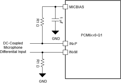
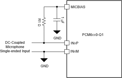
Figure 8-15 and Figure 8-16 show how to connect a DC-coupled microphone for a differential and single-ended input, respectively. The value of the external bias resistor, R1, must be appropriately chosen based upon the microphone impedance. For a differential input, the value of the external bias resistor is recommended to be used for half of the microphone impedance, whereas for a single-ended input, the external bias resistor is recommended to be the same as the microphone impedance.
 Figure 8-15 DC-Coupled Microphone Differential Input Connection
 Figure 8-16 DC-Coupled Microphone Single-Ended Input Connection
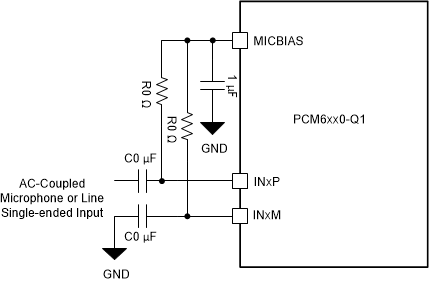
In AC-coupled mode, the value of the coupling capacitor must be so chosen that the high-pass filter formed by the coupling capacitor and the input impedance do not affect the signal content. At power-up, before proper recording can begin, this coupling capacitor must be charged up to the common-mode voltage. For single-ended input configuration, the INxM pin must be grounded after the AC coupling capacitor in AC-coupled mode.
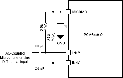
Figure 8-17 and Figure 8-18 show how to connect an AC-coupled microphone or line source for a differential and single-ended input, respectively. In AC-coupled mode, the device input pins INxP and INxM, must be biased appropriately for the DC common-mode value either using the on-chip MICBIAS output voltage along with external bias resistor, R0, or using an external bias generator circuit. The maximum value for resistor R0 depends upon the signal swing and the MICBIAS value programmed. See the PCM6xx0-Q1 AC Coupled External Resistor Calculator to calculate the R0 value for the desired system configuration.
 Figure 8-17 AC-Coupled Microphone or Line Differential Input Connection
 Figure 8-18 AC-Coupled Microphone or Line Single-Ended Input Connection