SBAS495D June 2010 – August 2021 PCM9211
PRODUCTION DATA
- 1 Features
- 2 Applications
- 3 Description
- 4 Revision History
- 5 Pin Configuration and Functions
-
6 Specifications
- 6.1 Absolute Maximum Ratings
- 6.2 ESD Ratings
- 6.3 Recommended Operating Conditions
- 6.4 Thermal Information
- 6.5 Electrical Characteristics: General
- 6.6 Electrical Characteristics: Analog-to-Digital Converter (ADC)
- 6.7 Electrical Characteristics: Digital Audio I/F Receiver (DIR)
- 6.8 Timing Requirements
- 6.9 Typical Characteristics: ADC
- 6.10 Typical Characteristics: ADC Internal Filter
- 6.11 Typical Characteristics: ADC Output Spectrum
-
7 Detailed Description
- 7.1 Overview
- 7.2 Functional Block Diagram
- 7.3
Feature Description
- 7.3.1 Digital Audio Interface Receiver (DIR)
- 7.3.2 Digital Audio Interface Transmitter (DIT)
- 7.3.3 Analog-to-Digital Converter (ADC)
- 7.3.4 Auxiliary PCM Audio Input and Output (I/O)
- 7.3.5 Routing
- 7.3.6 Control Interface
- 7.3.7 Multipurpose I/O
- 7.3.8
PCM9211 Module Descriptions
- 7.3.8.1 Power Supply
- 7.3.8.2 Power-Down Function
- 7.3.8.3 System Reset
- 7.3.8.4 PCM Audio Interface Format
- 7.3.8.5
ADC Details
- 7.3.8.5.1 System Clock
- 7.3.8.5.2 ADC: Clock Source Configuration
- 7.3.8.5.3 ADC: Standalone Operation
- 7.3.8.5.4 Additional ADC Functions
- 7.3.8.5.5 ADC: Power Down and Power Up
- 7.3.8.5.6 ADC: Audio Interface Mode and Timing
- 7.3.8.5.7 Audio Interface Format
- 7.3.8.5.8 ADC and Synchronization with Other Clocks
- 7.3.8.5.9 Setting the ADC Sampling Frequency with XTI as Clock Source
- 7.3.8.5.10 Analog Inputs to the ADC
- 7.3.8.5.11 VCOM Output
- 7.3.8.5.12 Oversampling Rate
- 7.3.8.5.13 External ADC Mode
- 7.3.8.5.14 ADC Level Detect and Interrupt
- 7.3.8.5.15 Real World Application
- 7.3.8.6
Digital Audio Interface Receiver (Rxin0 To Rxin11)
- 7.3.8.6.1 Input Details for Pins Rxin0 through Rxin11
- 7.3.8.6.2 PLL Clock Source (Built-In PLL and VCO) Details
- 7.3.8.6.3 DIR and PLL Loop Filter Details
- 7.3.8.6.4 External (XTI) Clocks, Oscillators, and Supporting Circuitry
- 7.3.8.6.5 DIR Data Description
- 7.3.8.6.6 Channel Status Data, User Data, and Validity Flag
- 7.3.8.6.7 DIR: Parity Error Processing
- 7.3.8.6.8 DIR: Errors and Interrupts
- 7.3.8.6.9 DIR: Sampling Frequency Calculator for Incoming S/PDIF Inputs
- 7.3.8.6.10 DIR: Audio Port Sampling Frequency Calculator
- 7.3.8.6.11 Output Register Construction
- 7.3.8.6.12 DIR: Auto Source Selector for Main Output and AUX Output
- 7.3.8.6.13 Non-PCM Data Detection
- 7.3.8.6.14 PC/PD Monitor
- 7.3.8.7 Digital Audio Interface Transmitter
- 7.3.8.8
MPIO Description
- 7.3.8.8.1 Overview
- 7.3.8.8.2 Assignable Signals for MPIO Pins
- 7.3.8.8.3 How to Assign Functions to MPIO
- 7.3.8.8.4 Selection of Output Source
- 7.3.8.8.5 Assignable Signals to MPO Pins
- 7.3.8.8.6 MPIO and MPO Assignments
- 7.3.8.8.7 MPIO Description
- 7.3.8.8.8 MPIO And MPO Assignment: Pin Assignment Details
- 7.3.8.9 Default Routing Function (After Reset)
- 7.3.8.10 Multichannel PCM Routing Function
- 7.4 Device Functional Modes
- 7.5
Register Maps
- 7.5.1 Error Output Condition and Shared Port Settings Register (address = 20h) [reset = 00000000]
- 7.5.2 DIR Initial Settings Register 1/3 (address: 21h) [reset = 00000000]
- 7.5.3 DIR Initial Settings Register 2/3 (address: 22h) [reset = 00000001]
- 7.5.4 DIR Initial Settings Register 3/3 (address: 23h) [reset = 00000100]
- 7.5.5 Oscillation Circuit Control Register (address: 24h) [reset = 00000000]
- 7.5.6 Error Cause Setting Register (address = 25h) [reset = 00000001]
- 7.5.7 AUTO Source Selector Cause Setting Register (address = 26h) [reset = 00000001]
- 7.5.8 DIR Acceptable fS Range Setting and Mask Register (address: 27h) [reset = 00000000]
- 7.5.9 Non-PCM Definition Register (address = 28h) [reset = 00000011]
- 7.5.10 DTS-CD/LD Sync Word and Period Detection Setting Register (address: 29h) [reset = 00001100]
- 7.5.11 INT0 Output Cause Mask Setting Register (Address: 2Ah) [reset = 11111111]
- 7.5.12 INT1 Output Cause Mask Setting Register (Address: 2Bh) [reset = 11111111]
- 7.5.13 INT0 Output Register (address = 2Ch) [reset = N/A]
- 7.5.14 INT1 Output Register (address = 2Dh) [reset = N/A]
- 7.5.15 INT0, INT1 Output Polarity Setting Register (address = 2Eh) [reset = 00000000]
- 7.5.16 DIR Output Data Format Register (address = 2Fh) [reset = 00000100]
- 7.5.17 DIR Recovered System Clock (SCK) Ratio Setting Register (address = 30h) [reset = 00000010]
- 7.5.18 XTI Source, Clock (SCK, BCK, LRCK) Frequency Setting Register (address = 31h) [reset = 00011010]
- 7.5.19 DIR Source, Secondary Bit/LR Clock (SBCK/SLRCK) Frequency Setting Register (address = 32h) [reset = 00100010]
- 7.5.20 XTI Source, Secondary Bit/LR Clock (SBCK/SLRCK) Frequency Setting Register (address = 33h) [reset = 00100010]
- 7.5.21 DIR Input Biphase Source Select, Coax Amplifier Control Register (address = 34h) [reset = 11000010]
- 7.5.22 RECOUT0 Output Biphase Source Settings Register (address = 35h) [reset = 00000010]
- 7.5.23 RECOUT1 Output Biphase Source Settings Register (address = 36h) [reset = 00000010]
- 7.5.24 Port Sampling Frequency Calculator Measurement Target Setting Register (address = 37h) [reset = 00000000]
- 7.5.25 Port Sampling Frequency Calculator Result Output Register (address = 38h) [reset = N/A]
- 7.5.26 Incoming Biphase Information and Sampling Frequency Register (address = 39h) [reset = N/A]
- 7.5.27 PC Buffer (Burst Preamble PC Output) Register (address = 3Ah) [reset = N/A]
- 7.5.28 PD Buffer (Burst Preamble PD Output) Register (address = 3Ch) [reset = N/A]
- 7.5.29 System Reset Control Register (address = 40h) [reset = 11000000]
- 7.5.30 ADC Function Control Register 1/3 (address = 42h) [reset = 00000010]
- 7.5.31 ADC L-Ch, Digital ATT Control Register (address = 46h) [reset = 11010111]
- 7.5.32 ADC R-Ch, Digital ATT Control Register (address = 47h) [reset = 11010111]
- 7.5.33 ADC Function Control Register 2/3 (address = 48h) [reset = 00000000]
- 7.5.34 ADC Function Control Register 3/3 (address = 49h) [reset = 00000000]
- 7.5.35 DIR Channel Status Data Buffer Register (address = 5Ah) [reset = 00000000]
- 7.5.36 DIT Function Control Register 1/3 (address = 60h) [reset = 01000100]
- 7.5.37 DIT Function Control Register 2/3 (address = 61h) [reset = 00010000]
- 7.5.38 DIT Function Control Register 3/3 (address = 62h) [reset = 00000000]
- 7.5.39 DIT Channel Status Data Buffer Register (address = 63h) [reset = 00000000]
- 7.5.40 Main Output and AUXOUT Port Control Register (address = 6A) [reset = 00000000]
- 7.5.41 Main Output Port (SCKO/BCK/LRCK/DOUT) Source Setting Register (address = 6Bh) [reset = 00000000]
- 7.5.42 AUX Output Port (AUXSCKO/AUXBCKO/AUXLRCKO/AUXDOUT) Source Setting Register (address = 6Ch) [reset = 00000000]
- 7.5.43 MPIO_B and Main Output Port Hi-Z Control Register (address = 6Dh) [reset = 00000000]
- 7.5.44 MPIO_C and MPIO_A Hi-Z Control Register (address = 6Eh) [reset = 00001111]
- 7.5.45 MPIO_A, MPIO_B, MPIO_C Group Function Assign Register (address = 6Fh) [reset = 01000000]
- 7.5.46 MPIO_A Flags or GPIO Assign Setting Register (address = 70h) [reset = 00000000]
- 7.5.47 MPIO_B, MPIO_C Flags or GPIO Assign Setting Register (address = 71h) [reset = 00000000]
- 7.5.48 MPIO_A1, MPIO_A0 Output Flag Select Register (address = 72h) [reset = 00000000]
- 7.5.49 MPIO_A3, MPIO_A0 Output Flag Select Register (address = 73h) [reset = 00000000]
- 7.5.50 MPIO_B1, MPIO_B0 Output Flag Select Register (address = 74h) [reset = 00000000]
- 7.5.51 MPIO_B3, MPIO_B2 Output Flag Select Register (address = 75h) [reset = 00000000]
- 7.5.52 MPIO_C1, MPIO_C0 Output Flag Select Register (address = 76h) [reset = 00000000]
- 7.5.53 MPIO_C3, MPIO_C2 Output Flag Select Register (address = 77h) [reset = 00000000]
- 7.5.54 MPO1, MPO0 Function Assign Setting Register (address = 78h) [reset = 00111101]
- 7.5.55 GPIO I/O Direction Control for MPIO_A, MPIO_B Register (address = 79h) [reset = 00000000]
- 7.5.56 GPIO I/O Direction Control for MPIO_C Register (address = 7Ah) [reset = 00000000]
- 7.5.57 GPIO Output Data Setting for MPIO_A, MPIO_B Register (address = 7Bh) [reset = 00000000]
- 7.5.58 GPIO Output Data Setting for MPIO_C Register (address = 7Ch) [reset = 00000000]
- 7.5.59 GPIO Input Data Register for MPIO_A, MPIO_B Register (address = 7Dh) [reset = N/A]
- 7.5.60 GPIO Input Data Register for MPIO_C Register (address = 7Eh) [reset = N/A]
- 8 Application and Implementation
- 9 Power Supply Recommendations
- 10Layout
- 11Device and Documentation Support
- 12Mechanical, Packaging, and Orderable Information
Package Options
Mechanical Data (Package|Pins)
- PT|48
Thermal pad, mechanical data (Package|Pins)
Orderable Information
6.10 Typical Characteristics: ADC Internal Filter
All specifications at TA = 25°C, VCCAD = 5 V, VDD = 3.3 V, fS = 48 kHz, SCK = 512fS, and 24-bit data, unless otherwise noted.
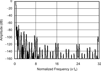
 Figure 6-5 Decimation Filter Stop Band Characteristic
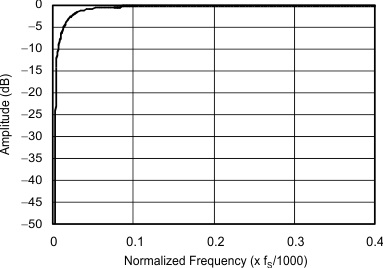
 Figure 6-7 High-Pass Filter Characteristic
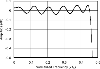
 Figure 6-6 Decimation Filter Passband Characteristic
 Figure 6-8 Antialiasing Filter Characteristic