SBASAH3A April 2022 – September 2022 PCMD3140-Q1
PRODUCTION DATA
- 1 Features
- 2 Applications
- 3 Description
- 4 Revision History
- 5 Pin Configuration and Functions
-
6 Specifications
- 6.1 Absolute Maximum Ratings
- 6.2 ESD Ratings
- 6.3 Recommended Operating Conditions
- 6.4 Thermal Information
- 6.5 Electrical Characteristics
- 6.6 Timing Requirements: I2C Interface
- 6.7 Switching Characteristics: I2C Interface
- 6.8 Timing Requirements: TDM, I2S or LJ Interface
- 6.9 Switching Characteristics: TDM, I2S or LJ Interface
- Timing Requirements: PDM Digital Microphone Interface
- 6.10 Switching Characteristics: PDM Digial Microphone Interface
- 6.11 Timing Diagrams
- 6.12 Typical Characteristics
-
7 Detailed Description
- 7.1 Overview
- 7.2 Functional Block Diagram
- 7.3
Feature Description
- 7.3.1 Serial Interfaces
- 7.3.2 Phase-Locked Loop (PLL) and Clock Generation
- 7.3.3 Reference Voltage
- 7.3.4 Microphone Bias
- 7.3.5 Digital PDM Microphone Record Channel
- 7.3.6
Signal-Chain Processing
- 7.3.6.1 Programmable Digital Volume Control
- 7.3.6.2 Programmable Channel Gain Calibration
- 7.3.6.3 Programmable Channel Phase Calibration
- 7.3.6.4 Programmable Digital High-Pass Filter
- 7.3.6.5 Programmable Digital Biquad Filters
- 7.3.6.6 Programmable Channel Summer and Digital Mixer
- 7.3.6.7
Configurable Digital Decimation Filters
- 7.3.6.7.1
Linear Phase Filters
- 7.3.6.7.1.1 Sampling Rate: 7.35 kHz to 8 kHz
- 7.3.6.7.1.2 Sampling Rate: 14.7 kHz to 16 kHz
- 7.3.6.7.1.3 Sampling Rate: 22.05 kHz to 24 kHz
- 7.3.6.7.1.4 Sampling Rate: 29.4 kHz to 32 kHz
- 7.3.6.7.1.5 Sampling Rate: 44.1 kHz to 48 kHz
- 7.3.6.7.1.6 Sampling Rate: 88.2 kHz to 96 kHz
- 7.3.6.7.1.7 Sampling Rate: 176.4 kHz to 192 kHz
- 7.3.6.7.1.8 Sampling Rate: 352.8 kHz to 384 kHz
- 7.3.6.7.1.9 Sampling Rate: 705.6 kHz to 768 kHz
- 7.3.6.7.2 Low-Latency Filters
- 7.3.6.7.3
Ultra-Low-Latency Filters
- 7.3.6.7.3.1 Sampling Rate: 14.7 kHz to 16 kHz
- 7.3.6.7.3.2 Sampling Rate: 22.05 kHz to 24 kHz
- 7.3.6.7.3.3 Sampling Rate: 29.4 kHz to 32 kHz
- 7.3.6.7.3.4 Sampling Rate: 44.1 kHz to 48 kHz
- 7.3.6.7.3.5 Sampling Rate: 88.2 kHz to 96 kHz
- 7.3.6.7.3.6 Sampling Rate: 176.4 kHz to 192 kHz
- 7.3.6.7.3.7 Sampling Rate: 352.8 kHz to 384 kHz
- 7.3.6.7.1
Linear Phase Filters
- 7.3.7 Voice Activity Detection (VAD)
- 7.3.8 Interrupts, Status, and Digital I/O Pin Multiplexing
- 7.4 Device Functional Modes
- 7.5 Programming
- 7.6 Register Maps
- 8 Application and Implementation
- 9 Power Supply Recommendations
- 10Layout
- 11Device and Documentation Support
- 12Mechanical, Packaging, and Orderable Information
Package Options
Mechanical Data (Package|Pins)
- RTE|20
Thermal pad, mechanical data (Package|Pins)
Orderable Information
3 Description
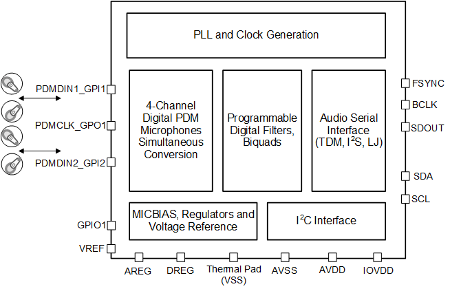
The PCMD3140-Q1 is a high-performance, pulse-density-modulation (PDM) input to time-division multiplexing (TDM) or I2S output converter that supports simultaneous sampling of up to four digital channels for the PDM microphone input. The device integrates programable digital volume control, a microphone bias voltage, a phase-locked loop (PLL), a programmable high-pass filter (HPF), biquad filters, low-latency filter modes, and allows for output sample rates up to 768 kHz. The device supports time-division multiplexing (TDM), I2S, or left-justified (LJ) audio formats, and can be controlled with the I2C interface. Additionally, the PCMD3140-Q1 supports master and slave mode selection for the audio bus interface operation. These integrated high-performance features, along with the ability to be powered from a single-supply of 3.3 V or 1.8 V, make the device an excellent choice for space-constrained audio systems in far-field microphone recording applications.
The PCMD3140-Q1 is specified from –40°C to +125°C, and is offered in a 20-pin WQFN package.
| PART NUMBER(1) | PACKAGE | BODY SIZE (NOM) |
|---|---|---|
| PCMD3140-Q1 | WQFN (20) | 3.00 mm × 3.00 mm with 0.5-mm pitch |
 Simplified Block Diagram