SBASAH3A April 2022 – September 2022 PCMD3140-Q1
PRODUCTION DATA
- 1 Features
- 2 Applications
- 3 Description
- 4 Revision History
- 5 Pin Configuration and Functions
-
6 Specifications
- 6.1 Absolute Maximum Ratings
- 6.2 ESD Ratings
- 6.3 Recommended Operating Conditions
- 6.4 Thermal Information
- 6.5 Electrical Characteristics
- 6.6 Timing Requirements: I2C Interface
- 6.7 Switching Characteristics: I2C Interface
- 6.8 Timing Requirements: TDM, I2S or LJ Interface
- 6.9 Switching Characteristics: TDM, I2S or LJ Interface
- Timing Requirements: PDM Digital Microphone Interface
- 6.10 Switching Characteristics: PDM Digial Microphone Interface
- 6.11 Timing Diagrams
- 6.12 Typical Characteristics
-
7 Detailed Description
- 7.1 Overview
- 7.2 Functional Block Diagram
- 7.3
Feature Description
- 7.3.1 Serial Interfaces
- 7.3.2 Phase-Locked Loop (PLL) and Clock Generation
- 7.3.3 Reference Voltage
- 7.3.4 Microphone Bias
- 7.3.5 Digital PDM Microphone Record Channel
- 7.3.6
Signal-Chain Processing
- 7.3.6.1 Programmable Digital Volume Control
- 7.3.6.2 Programmable Channel Gain Calibration
- 7.3.6.3 Programmable Channel Phase Calibration
- 7.3.6.4 Programmable Digital High-Pass Filter
- 7.3.6.5 Programmable Digital Biquad Filters
- 7.3.6.6 Programmable Channel Summer and Digital Mixer
- 7.3.6.7
Configurable Digital Decimation Filters
- 7.3.6.7.1
Linear Phase Filters
- 7.3.6.7.1.1 Sampling Rate: 7.35 kHz to 8 kHz
- 7.3.6.7.1.2 Sampling Rate: 14.7 kHz to 16 kHz
- 7.3.6.7.1.3 Sampling Rate: 22.05 kHz to 24 kHz
- 7.3.6.7.1.4 Sampling Rate: 29.4 kHz to 32 kHz
- 7.3.6.7.1.5 Sampling Rate: 44.1 kHz to 48 kHz
- 7.3.6.7.1.6 Sampling Rate: 88.2 kHz to 96 kHz
- 7.3.6.7.1.7 Sampling Rate: 176.4 kHz to 192 kHz
- 7.3.6.7.1.8 Sampling Rate: 352.8 kHz to 384 kHz
- 7.3.6.7.1.9 Sampling Rate: 705.6 kHz to 768 kHz
- 7.3.6.7.2 Low-Latency Filters
- 7.3.6.7.3
Ultra-Low-Latency Filters
- 7.3.6.7.3.1 Sampling Rate: 14.7 kHz to 16 kHz
- 7.3.6.7.3.2 Sampling Rate: 22.05 kHz to 24 kHz
- 7.3.6.7.3.3 Sampling Rate: 29.4 kHz to 32 kHz
- 7.3.6.7.3.4 Sampling Rate: 44.1 kHz to 48 kHz
- 7.3.6.7.3.5 Sampling Rate: 88.2 kHz to 96 kHz
- 7.3.6.7.3.6 Sampling Rate: 176.4 kHz to 192 kHz
- 7.3.6.7.3.7 Sampling Rate: 352.8 kHz to 384 kHz
- 7.3.6.7.1
Linear Phase Filters
- 7.3.7 Voice Activity Detection (VAD)
- 7.3.8 Interrupts, Status, and Digital I/O Pin Multiplexing
- 7.4 Device Functional Modes
- 7.5 Programming
- 7.6 Register Maps
- 8 Application and Implementation
- 9 Power Supply Recommendations
- 10Layout
- 11Device and Documentation Support
- 12Mechanical, Packaging, and Orderable Information
Package Options
Mechanical Data (Package|Pins)
- RTE|20
Thermal pad, mechanical data (Package|Pins)
Orderable Information
7.3.6 Signal-Chain Processing
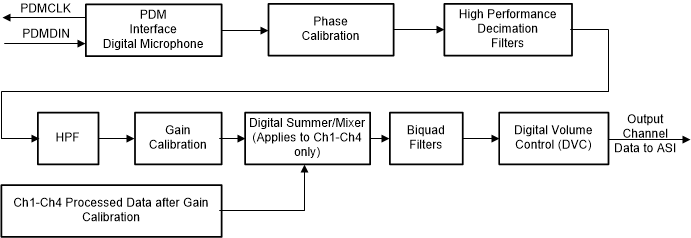
The PCMD3140-Q1 signal chain is comprised of high-performance, low-power, and highly flexible and programmable digital processing blocks. The high performance and flexibility combined with a compact package makes the PCMD3140-Q1 optimized for a wide variety of end-equipment and applications that require multichannel audio capture. Figure 7-16 shows a conceptual block diagram that highlights the various building blocks used in the signal chain, and how the blocks interact in the signal chain.
 Figure 7-16 Signal-Chain Processing Flowchart
The device supports up to four digital PDM microphone recording channels for simultaneous operation. The signal chain consists of various highly programmable digital processing blocks such as phase calibration, gain calibration, high-pass filter, digital summer or mixer, biquad filters, and volume control. The details on these processing blocks are discussed further in this section. Channels 1 to 4 in the signal chain block diagram of Figure 7-16 are as described in this section.
The desired input channels for recording can be enabled or disabled by using the IN_CH_EN (P0_R115) register, and the output channels for the audio serial interface can be enabled or disabled by using the ASI_OUT_EN (P0_R116) register. In general, the device supports simultaneous power-up and power-down of all active channels for simultaneous recording. However, based on the application needs, if some channels must be powered-up or powered-down dynamically when the other channel recording is on, then that use case is supported by setting the DYN_CH_PUPD_EN (P0_R117_D4) register bit to 1'b1 but do not power-down channel 1 in this mode of operation.
The device supports an input signal bandwidth up to 80 kHz, which allows the high-frequency non-audio signal to be recorded by using a 176.4-kHz (or higher) sample rate.
For output sample rates of 48 kHz or lower, the device supports all features for 4-channel recording and various programmable processing blocks. However, for output sample rates higher than 48 kHz, there are limitations in the number of simultaneous channel recordings supported and the number of biquad filters and such. See the TLV320ADCx120 Sampling Rates and Programmable Processing Blocks Supported application report for further details.