SLASEJ4C April 2017 – February 2023 PGA460
PRODUCTION DATA
- 1 Features
- 2 Applications
- 3 Description
- 4 Revision History
- 5 Pin Configuration and Functions
-
6 Specifications
- 6.1 Absolute Maximum Ratings
- 6.2 ESD Ratings
- 6.3 Recommended Operating Conditions
- 6.4 Thermal Information
- 6.5 Internal Supply Regulators Characteristics
- 6.6 Transducer Driver Characteristics
- 6.7 Transducer Receiver Characteristics
- 6.8 Analog to Digital Converter Characteristics
- 6.9 Digital Signal Processing Characteristics
- 6.10 Temperature Sensor Characteristics
- 6.11 High-Voltage I/O Characteristics
- 6.12 Digital I/O Characteristics
- 6.13 EEPROM Characteristics
- 6.14 Timing Requirements
- 6.15 Switching Characteristics
- 6.16 Typical Characteristics
-
7 Detailed Description
- 7.1 Overview
- 7.2 Functional Block Diagram
- 7.3
Feature Description
- 7.3.1 Power-Supply Block
- 7.3.2 Burst Generation
- 7.3.3 Analog Front-End
- 7.3.4 Digital Signal Processing
- 7.3.5 System Diagnostics
- 7.3.6
Interface Description
- 7.3.6.1 Time-Command Interface
- 7.3.6.2
USART Interface
- 7.3.6.2.1 USART Asynchronous Mode
- 7.3.6.2.2 One-Wire UART Interface
- 7.3.6.2.3 Ultrasonic Object Detection Through UART Operations
- 7.3.6.3 In-System IO-Pin Interface Selection
- 7.3.7 Echo Data Dump
- 7.3.8 Low-Power Mode
- 7.3.9 Transducer Time and Temperature Decoupling
- 7.3.10 Memory CRC Calculation
- 7.3.11 Temperature Sensor and Temperature Data-Path
- 7.3.12 TEST Pin Functionality
- 7.4 Device Functional Modes
- 7.5 Programming
- 7.6 Register Maps
- 8 Application and Implementation
- 9 Device and Documentation Support
- 10Mechanical, Packaging, and Orderable Information
Package Options
Mechanical Data (Package|Pins)
- PW|16
Thermal pad, mechanical data (Package|Pins)
Orderable Information
7.3.7.2 Direct Data Burst Through USART Synchronous Mode
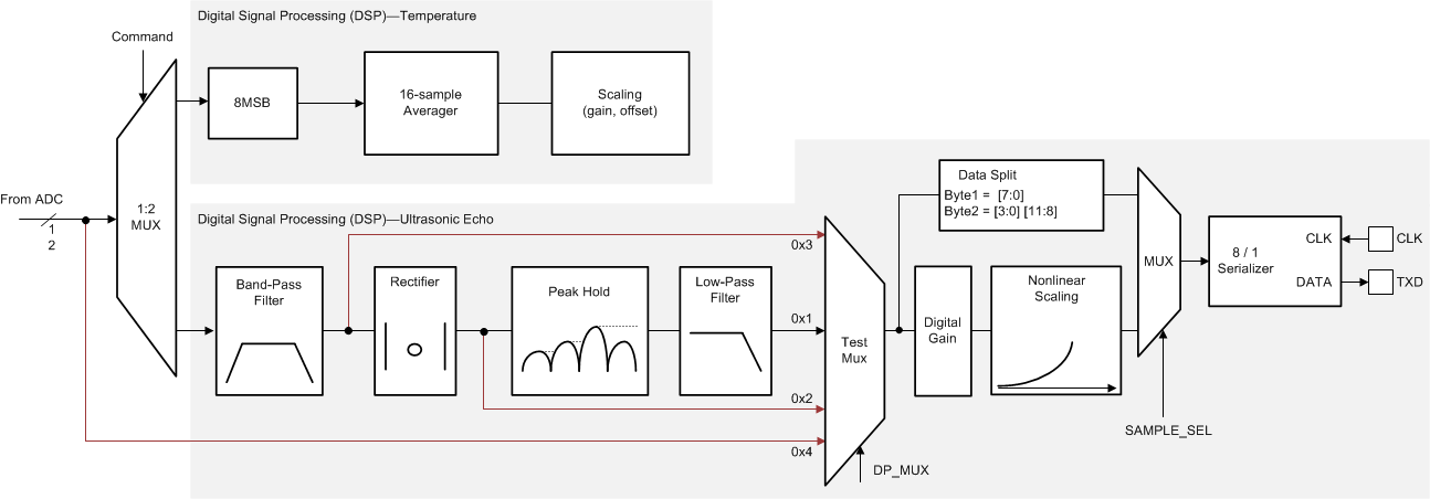
In the case where each 1-µs Data-Path sample must be extracted for further analysis, the PGA460 device offers a Test Mode where the Raw Digital data can be extracted at different points in the Digital data path (see #X3721). Data burst is enabled when DP_MUX value is greater than 0 and less than 5, then the object detection and measurement is disabled.

To enable this mode, the Digital Data-Path Mux can select the source signal to be burst out of the device by setting the DP_MUX parameter in the device memory. Once the DP_MUX parameter is enabled (set to a value other than 0x00), and if any of the SEND/RECEIVE, Receive Only or TEMPERATURE READ commands are issued using the standard UART command method, the selected source signal is passed through the Digital Multiplexer and Serialized by the 8/1 Serializer block. This signal is immediately outputted on the UART TXD pin that now acts as a data output pin, while the controller sends clock pulses to the CLK pin.
It is important that after issuing any of these commands the controller does not stop sending clock pulses on the CLK pin until the Bus is idle. Once a Checksum received is verified and the bus is idle, that is considered the end of the Burst data. This is needed for proper data synchronization in the PGA460 device. For further explanation on the USART Synchronous communication mode, see the GUID-B377F31E-83E5-43D0-AD45-7BF3C64AD86B.html#TITLE-SLASEC8X4567 section.
#X2814 shows the format of the order of the data stream coming out of the PGA460 device.
As shown in #X2814, the output data-stream starts with a PGA460 diagnostic data field, followed by number of data bytes and ends with a checksum field calculated on the diagnostic data byte and all data bytes. The number of data bytes depends on the number of samples extracted from the PGA460 device, which depends on the Recording Time Interval of the current command. The recording time Interval is determined by the P1_REC and P2_REC parameters in the EEPROM memory while the sampling rate of the ADC and digital signal path is 1 µs / Sample. From here it can be calculated that the number of samples is equivalent to the recording time when expressed in microseconds.
The digital output offers two modes of operation based on the SAMPLE_SEL parameter:
- When SAMPLE_SEL = 0The output of the data path is selected by the Digital Data-Path Test Mux and the data length is 8 bits/sample long. For the LPF output , we now use the active digital gain select to determine which 8 bits are sent out. For all the others, if the active digital gain select = 0 then we get the 8 MSB bits, else the PGA460 sends the 8 LSB bits. In this case, the sample rate is 1us, meaning every sample that the ADC outputs will also be sent out of the PGA460 device.
- When SAMPLE_SEL = 1The output of the data path is selected by the digital data path test mux. However, the full 12bits/sample data length is sent out of the PGA460 device. In this case, the sample rate is 2 µs, meaning every 2nd sample produced by the ADC will be sent out. The 12 bit data is split into two bytes and sent in the order LS Byte followed by the MS Byte. The MS Byte is padded with a 4 bit sample counter so that the controller can track the order of samples from the PGA460 device.
For both of the previously listed options, the nonlinear scaling block is only enabled if the data is extracted from the Low-Pass filter (DP_MUX = 0x1). In all other cases, the nonlinear scaling block is disabled.