SLTS278J November 2010 – March 2020 PTH08T250W
PRODUCTION DATA.
- 1 Features
- 2 Applications
- 3 Description
- 4 Revision History
- 5 Description (continued)
- 6 Pin Configuration and Functions
- 7 Specifications
- 8 Detailed Description
-
9 Application and Implementation
- 9.1
Typical Application
- 9.1.1
Detailed Design Procedure
- 9.1.1.1 Adjusting the Output Voltage
- 9.1.1.2
Capacitor Recommendations for the PTH08T250W Power Module
- 9.1.1.2.1 Capacitor Technologies
- 9.1.1.2.2 Input Capacitor (Required)
- 9.1.1.2.3 Input Capacitor Information
- 9.1.1.2.4 Output Capacitor (Required)
- 9.1.1.2.5 Output Capacitor Information
- 9.1.1.2.6 TurboTrans Output Capacitance
- 9.1.1.2.7 Non-TurboTrans Output Capacitance
- 9.1.1.2.8 Designing for Fast Load Transients
- 9.1.1.2.9 Capacitor Table
- 9.1.1.3 TurboTrans™ Technology
- 9.1.1.4 TurboTrans™ Selection
- 9.1.1.5 Undervoltage Lockout (UVLO)
- 9.1.1.6 On/Off Inhibit
- 9.1.1.7 Current Sharing
- 9.1.1.8 Prebias Startup Capability
- 9.1.1.9 SmartSync Technology
- 9.1.1.10 Auto-Track™ Function
- 9.1.1
Detailed Design Procedure
- 9.1
Typical Application
- 10Device and Documentation Support
- 11Mechanical, Packaging, and Orderable Information
Package Options
Refer to the PDF data sheet for device specific package drawings
Mechanical Data (Package|Pins)
- BCU|22
- ECT|22
- ECU|22
Thermal pad, mechanical data (Package|Pins)
Orderable Information
9.1.1.7.1.2 Current Sharing Layout
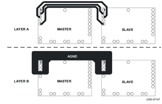
In current sharing applications the VI pins of both modules must be connected to the same input bus. The VO pins of both modules are connected together to power the load. The GND pins of both modules are connected via the GND plane. Four other inter-connection pins are connected between the modules. Figure 27 shows the required layout of the inter-connection pins for two modules configured to share current. Notice that the Share (pin 2) connection is routed between the Comp (pin 3) and CLKIO (pin 5) connections. AGND (pin 4) should be connected as a thicker trace on an adjacent layer, running parallel to pins 2, 3 and 5. AGND must not be connected to the GND plane.
 Figure 27. Recommended Layout of Inter-Connection Pins Between Two Current Sharing Modules