SLTS278J November 2010 – March 2020 PTH08T250W
PRODUCTION DATA.
- 1 Features
- 2 Applications
- 3 Description
- 4 Revision History
- 5 Description (continued)
- 6 Pin Configuration and Functions
- 7 Specifications
- 8 Detailed Description
-
9 Application and Implementation
- 9.1
Typical Application
- 9.1.1
Detailed Design Procedure
- 9.1.1.1 Adjusting the Output Voltage
- 9.1.1.2
Capacitor Recommendations for the PTH08T250W Power Module
- 9.1.1.2.1 Capacitor Technologies
- 9.1.1.2.2 Input Capacitor (Required)
- 9.1.1.2.3 Input Capacitor Information
- 9.1.1.2.4 Output Capacitor (Required)
- 9.1.1.2.5 Output Capacitor Information
- 9.1.1.2.6 TurboTrans Output Capacitance
- 9.1.1.2.7 Non-TurboTrans Output Capacitance
- 9.1.1.2.8 Designing for Fast Load Transients
- 9.1.1.2.9 Capacitor Table
- 9.1.1.3 TurboTrans™ Technology
- 9.1.1.4 TurboTrans™ Selection
- 9.1.1.5 Undervoltage Lockout (UVLO)
- 9.1.1.6 On/Off Inhibit
- 9.1.1.7 Current Sharing
- 9.1.1.8 Prebias Startup Capability
- 9.1.1.9 SmartSync Technology
- 9.1.1.10 Auto-Track™ Function
- 9.1.1
Detailed Design Procedure
- 9.1
Typical Application
- 10Device and Documentation Support
- 11Mechanical, Packaging, and Orderable Information
Package Options
Refer to the PDF data sheet for device specific package drawings
Mechanical Data (Package|Pins)
- BCU|22
- ECT|22
- ECU|22
Thermal pad, mechanical data (Package|Pins)
Orderable Information
9.1.1.9 SmartSync Technology
SmartSync technology allows multiple power modules to be synchronized to a common frequency. When not used, this pin must be connect to GND. Driving the SmartSync pins with an external oscillator set to the desired frequency, synchronizes all connected modules to the selected frequency. The synchronization frequency can be higher or lower than the nominal switching frequency of the modules within the range of 240 kHz to 400 kHz.
Synchronizing modules powered from the same bus eliminates beat frequencies reflected back to the input supply, and also reduces EMI filtering requirements. Eliminating the low beat frequencies (usually <10 kHz) allows the EMI filter to be designed to attenuate only the synchronization frequency. Power modules can also be synchronized out-of-phase to minimize ripple current and reduce input capacitance requirements.
NOTE
The PTH08T250W requires that the external synchronization frequency be present before a valid input voltage is present or before release of the inhibit control.
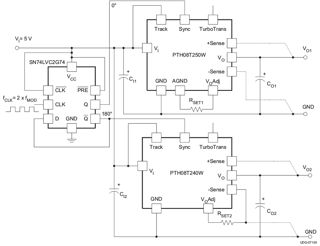
Figure 30 shows a standard circuit with two modules synchronized 180° out-of-phase using a D flip-flop circuit.
 Figure 30. Typical SmartSync Schematic
 Operating the PTH08T250W with a low duty cycle may increase the output voltage ripple. When operating at the nominal switching frequency, input voltages greater than (VO × 12) may cause the output voltage ripple to increase (up to 2×).
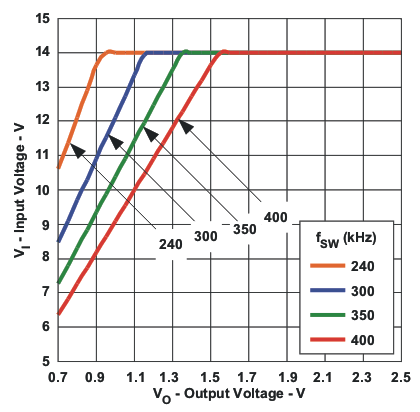
When using Smart Sync, the minimum duty cycle varies as a function of output voltage and switching frequency. Synchronizing to a higher frequency causes greater restrictions on the duty cycle range. For a given switching frequency, Figure 31 shows the operating region where the output voltage ripple meets the electrical specifications. Operation above a given curve may cause the output voltage ripple to increase (up to 2×). For example, a module operating at 400 kHz and an output voltage of 1.2 V, the maximum input voltage that meets the output voltage ripple specification is 11 V. Exceeding 11 V may cause in an increase in output voltage ripple. As shown in Figure 31, operating below 6 V allows operation down to the minimum output voltage over the entire synchronization frequency range without affecting the output voltage ripple. See the Electrical Characteristics table for the synchronization frequency range limits.
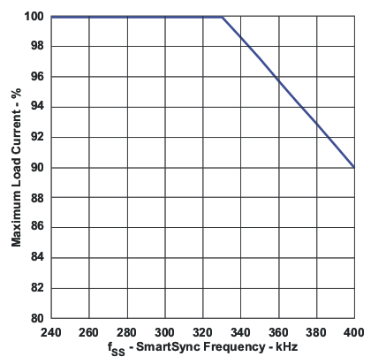
The maximum output current that a single module can deliver may also be affected by the sychronization frequency. See Figure 32 below for load current derating when sychronizing at frequencies greater than 330 kHz. First consult the temperature derating graphs in the Typical Characteristics section to determine the maximum output current based on operating conditions. Any derating due to the SmartSync frequency is in addition to the temperature derating.
 Figure 31. Output Voltage Ripple Limits
  Figure 32. Maximum Load Current versus SmartSync Frequency