SLOS412E April 2003 – November 2024 RC4580
PRODUCTION DATA
- 1
- 1 Features
- 2 Applications
- 3 Description
- 4 Pin Configuration and Functions
- 5 Specifications
- 6 Detailed Description
- 7 Application and Implementation
- 8 Device and Documentation Support
- 9 Revision History
- 10Mechanical, Packaging, and Orderable Information
Package Options
Refer to the PDF data sheet for device specific package drawings
Mechanical Data (Package|Pins)
- D|8
- P|8
- DDF|8
- DGK|8
- PW|8
Thermal pad, mechanical data (Package|Pins)
Orderable Information
7.1 Typical Application
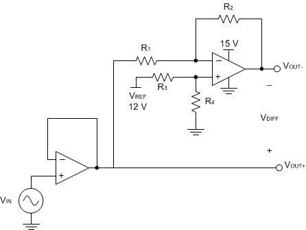
Some applications require differential signals. Figure 7-1 shows a simple circuit to convert a single-ended input of 2V to 10V into differential output of ±8V on a single 15V supply. The output range is intentionally limited to maximize linearity. The circuit is composed of two amplifiers. One amplifier acts as a buffer and creates a voltage, VOUT+. The second amplifier inverts the input and adds a reference voltage to generate VOUT–. Both VOUT+ and VOUT– range from 2V to 10V. The difference, VDIFF, is the difference between VOUT+ and VOUT–.
 Figure 7-1 Schematic for Single-Ended Input to Differential Output Conversion