-
REF1112 10ppm/°C, 1μA, 1.25V Shunt Voltage Reference
- 1
- 1 Features
- 2 Applications
- 3 Description
- 4 Pin Configuration and Functions
- 5 Specifications
- 6 Detailed Description
-
7 Application and Implementation
- 7.1 Application Information
- 7.2 Typical Applications
- 7.3 Power Supply Recommendations
- 7.4 Layout
- 8 Device and Documentation Support
- 9 Revision History
- 10Mechanical, Packaging, and Orderable Information
- IMPORTANT NOTICE
Package Options
Mechanical Data (Package|Pins)
- DBZ|3
Thermal pad, mechanical data (Package|Pins)
Orderable Information
Data Sheet
REF1112 10ppm/°C, 1μA, 1.25V Shunt Voltage Reference
1 Features
- Small package: SOT23-3
- Fixed reverse breakdown voltage of 1.25V
- Key specifications
- Output voltage tolerance: ±0.2% (maximum)
- Low output noise (0.1Hz to 10Hz): 25μVpp (typical)
- Temperature range: −40°C to +125°C
- Operating current range: 1.2μA to 5mA
- Low temperature coefficient from 0°C to +70°C: 30ppm/°C (maximum)
- Low temperature coefficient from –40°C to +85°C: 50ppm/°C (maximum)
2 Applications
- Battery-powered instruments
- Building security sensors
- Medical equipment
- Field transmitters
- Calibrators
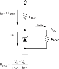
 Shunt Reference Application Schematic
3 Description
The REF1112 device is a two-terminal shunt reference designed for power and space sensitive applications. The REF1112 features an operating current of 1μA in a SOT23-3 package and is an improved, lower power voltage reference for designs currently using voltage references in larger packages, such as the REF1004 and LT1004. The REF1112 is specified from –40°C to +85°C with operation extending from –40°C to +125°C.
The REF1112 complements other 1μA components from Texas Instruments including the OPA349 and TLV240x low-power operational amplifiers, and the TLV349x micropower voltage comparator.
(1) For all available packages, see the orderable addendum at the
end of the data sheet.
(2) The package size (length × width) is a nominal value and includes pins,
where applicable.
ㅤ
ㅤ
ㅤ
ㅤ
ㅤ

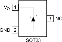
A. NC indicates the pin must be left
unconnected or connected to GND
Pinout