SBOS392H August   2007  – August 2019 REF3312 , REF3318 , REF3320 , REF3325 , REF3330 , REF3333

PRODUCTION DATA.  

  1. Features
  2. Applications
  3. Description
    1.     Device Images
      1.      REF3312 in a Single-Supply Signal Chain
      2.      Dropout Voltage vs Load Current
  4. Revision History
  5. Device Comparison
  6. Pin Configuration and Functions
    1. Table 1. Pin Functions
  7. Specifications
    1. 7.1 Absolute Maximum Ratings
    2. 7.2 ESD Ratings
    3. 7.3 Recommended Operating Conditions
    4. 7.4 Thermal Information
    5. 7.5 Electrical Characteristics
    6. 7.6 Typical Characteristics
  8. Parameter Measurement Information
    1. 8.1 Thermal Hysteresis
  9. Detailed Description
    1. 9.1 Overview
    2. 9.2 Functional Block Diagram
    3. 9.3 Feature Description
      1. 9.3.1 Start-Up Time
      2. 9.3.2 Low Temperature Drift
      3. 9.3.3 Power Dissipation
      4. 9.3.4 Noise Performance
    4. 9.4 Device Functional Modes
  10. 10Applications and Implementation
    1. 10.1 Application Information
    2. 10.2 Typical Applications
      1. 10.2.1 REF3312 in a Bipolar Signal-Chain Configuration
        1. 10.2.1.1 Design Requirements
        2. 10.2.1.2 Detailed Design Procedure
          1. 10.2.1.2.1 Op Amp Level-Shift Design
          2. 10.2.1.2.2 Differential Input Attenuator Design
          3. 10.2.1.2.3 Input Filtering
          4. 10.2.1.2.4 Component Selection
            1. 10.2.1.2.4.1 Voltage References
            2. 10.2.1.2.4.2 Op Amp
          5. 10.2.1.2.5 Input Attenuation and Level Shifting
          6. 10.2.1.2.6 Input Filtering
          7. 10.2.1.2.7 Passive Component Tolerances and Materials
        3. 10.2.1.3 Application Curves
          1. 10.2.1.3.1 DC Performance
          2. 10.2.1.3.2 AC Performance
  11. 11Power-Supply Recommendations
  12. 12Layout
    1. 12.1 Layout Guidelines
    2. 12.2 Layout Example
  13. 13Device and Documentation Support
    1. 13.1 Documentation Support
      1. 13.1.1 Related Documentation
    2. 13.2 Related Links
    3. 13.3 Receiving Notification of Documentation Updates
    4. 13.4 Community Resources
    5. 13.5 Trademarks
    6. 13.6 Electrostatic Discharge Caution
    7. 13.7 Glossary
  14. 14Mechanical, Packaging, and Orderable Information

Package Options

Mechanical Data (Package|Pins)
Thermal pad, mechanical data (Package|Pins)
Orderable Information

Pin Configuration and Functions

REF3312, REF3318, REF3320, REF3325, REF3330, REF3333
DBZ Package and DCK Package
SOT-23-3, SC70-3
(Top View)
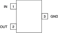
REF3312 REF3318 REF3320 REF3325 REF3330 REF3333 po_bos392.gif
REF3312, REF3318, REF3320, REF3325, REF3330, REF3333
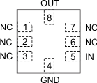
RSE Package
UQFN-8
(Top View)
REF3312 REF3318 REF3320 REF3325 REF3330 REF3333 po_rse_uqfn-8_bos392.gif

Table 1. Pin Functions

PIN DESCRIPTION
NAME DBZ, DCK RSE
GND 3 4 Ground
IN 1 5 Input supply voltage
NC 1, 2, 3, 6, 7 Not connected
OUT 2 8 Output voltage