SBAS804F September 2017 – June 2021 REF3425 , REF3430 , REF3433 , REF3440 , REF3450
PRODUCTION DATA
- 1 Features
- 2 Applications
- 3 Description
- 4 Revision History
- 5 Device Comparison Table
- 6 Pin Configuration and Functions
- 7 Specifications
- 8 Parameter Measurement Information
- 9 Detailed Description
- 10Application and Implementation
- 11Power Supply Recommendations
- 12Layout
- 13Device and Documentation Support
- 14Mechanical, Packaging, and Orderable Information
Package Options
Mechanical Data (Package|Pins)
- DBV|6
Thermal pad, mechanical data (Package|Pins)
Orderable Information
3 Description
The REF34xx device is a low temperature drift
(6 ppm/°C), low-power, high-precision CMOS voltage
reference, featuring ±0.05% initial accuracy, low operating current with power
consumption less than 95 μA. This device also offers very low output noise of 3.8
μVp-p /V, which enables its ability to maintain high signal integrity
with high-resolution data converters in noise critical systems. With a small SOT-23
package, REF34xx offers enhanced specifications and pin-to-pin replacement for
MAX607x, ADR34xx and LT1790 (REF34xxT, no EN pin). The REF34xx family is compatible
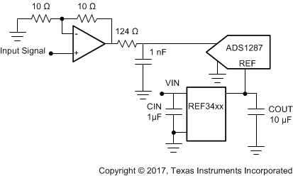
to most of the ADC and DAC such as ADS1287, DAC8802 and ADS1112.
Stability and system reliability are further improved by the low output-voltage hysteresis of the device and low long-term output voltage drift. Furthermore, the small size and low operating current of the devices (95 μA) benefit portable and battery-powered applications.
REF34xx is specified for the wide temperature range of −40°C to +125°C.
| PART NAME | PACKAGE (1) | BODY SIZE (NOM) |
|---|---|---|
REF34xx REF34xxT |
SOT-23 (6) | 2.90 mm × 1.60 mm |
 Simplified Schematic
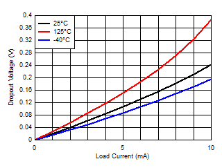
 Dropout vs. Current Load Over Temperature